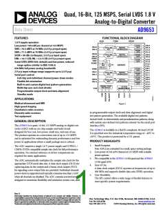
AD9653
Data Sheet
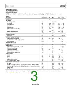
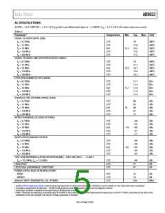
AVDD = 1.8 V, DRVDD = 1.8 V, 2.6 V p-p full-scale differential input at −1.0 dBFS; VREF = 1.3 V; 0°C to 85°C, DCS off, unless otherwise noted.
Table 2.
Parameter1
Temperature Min
Typ
Max Unit
RESOLUTION
16
Bits
ACCURACY
No Missing Codes
Offset Error
Offset Matching
Gain Error
25°C
25°C
25°C
25°C
25°C
25°C
25°C
Guaranteed
−0.3
+0.2
−5
1.1
0.8
% FSR
% FSR
% FSR
% FSR
LSB
Gain Matching
Differential Nonlinearity (DNL)
Integral Nonlinearity (INL)
TEMPERATURE DRIFT
Offset Error
5.0
LSB
25°C
3.5
ppm/°C
INTERNAL VOLTAGE REFERENCE
Output Voltage (1.3 V Programmable Mode)
Load Regulation at 1.0 mA (VREF = 1.3 V)
Input Resistance
25°C
25°C
25°C
1.3
6.5
7.5
V
mV
kΩ
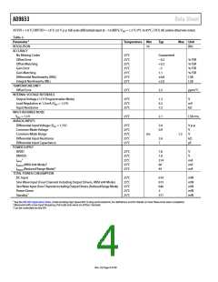
INPUT-REFERRED NOISE
VREF = 1.3 V
25°C
2.1
LSB rms
ANALOG INPUTS
Differential Input Voltage (VREF = 1.3 V)
Common-Mode Voltage
Common-Mode Range
Differential Input Resistance
Differential Input Capacitance
POWER SUPPLY
25°C
25°C
25°C
25°C
25°C
2.6
0.9
V p-p
V
V
kΩ
pF
0.6
1.3
2.6
7
AVDD
25°C
25°C
25°C
25°C
25°C
1.8
1.8
314
60
V
V
mA
mA
mA
DRVDD
2
IAVDD
IDRVDD (ANSI-644 Mode)2
IDRVDD (Reduced Range Mode)2
45
TOTAL POWER CONSUMPTION
DC Input
25°C
25°C
25°C
25°C
25°C
614
673
646
2
mW
mW
mW
mW
mW
Sine Wave Input (Four Channels Including Output Drivers, ANSI-644 Mode)
Sine Wave Input (Four Channels Including Output Drivers, Reduced Range Mode)
Power-Down
Standby3
371
1 See the AN-835 Application Note, Understanding High Speed ADC Testing and Evaluation, for definitions and for details on how these tests were completed.
2 Measured with a low input frequency, full-scale sine wave on all four channels.
3 Can be controlled via the SPI.
Rev. 0 | Page 4 of 40

 ADI [ ADI ]