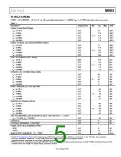
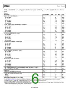
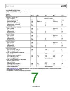
Data Sheet
AD9653
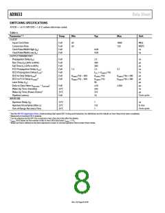
TIMING SPECIFICATIONS
Table 7.
Unit
Parameter
Description
Limit
SYNC TIMING REQUIREMENTS
tSSYNC
tHSYNC
SYNC to rising edge of CLK+ setup time
SYNC to rising edge of CLK+ hold time
See Figure 75
0.24
0.40
ns typ
ns typ
SPI TIMING REQUIREMENTS
tDS
tDH
tCLK
tS
tH
tHIGH
tLOW
tEN_SDIO
Setup time between the data and the rising edge of SCLK
Hold time between the data and the rising edge of SCLK
Period of the SCLK
Setup time between CSB and SCLK
Hold time between CSB and SCLK
SCLK pulse width high
SCLK pulse width low
Time required for the SDIO pin to switch from an input to an output relative to the
SCLK falling edge (not shown in Figure 75)
2
2
40
2
2
10
10
10
ns min
ns min
ns min
ns min
ns min
ns min
ns min
ns min
tDIS_SDIO
Time required for the SDIO pin to switch from an output to an input relative to the
SCLK rising edge (not shown in Figure 75)
10
ns min
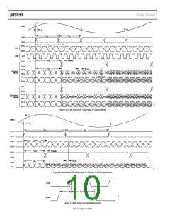
Timing Diagrams
Refer to the Memory Map Register Descriptions section and Table 23 for SPI register settings.
N – 1
VIN±x
N
N + 1
tA
tEH
tEL
CLK–
CLK+
DCO–
tCPD
DDR
SDR
DCO+
DCO
tFCO
tFRAME
FCO–
FCO+
D0–A
tPD
tDATA
BITWISE
MODE
D14
D12
D10
D08
D06
D04
D02
LSB
D14
D12
D10
D08
D06
D04
D02
LSB
N – 17 N – 17 N – 17 N – 17 N – 17 N – 17 N – 17 N – 17 N – 16 N – 16 N – 16 N – 16 N – 16 N – 16 N – 16 N – 16
D0+A
D1–A
tLD
MSB
D13
D11
D09
D07
D05
D03
D01
MSB
D13
D11
D09
D07
D05
D03
D01
N – 17 N – 17 N – 17 N – 17 N – 17 N – 17 N – 17 N – 17 N – 16 N – 16 N – 16 N – 16 N – 16 N – 16 N – 16 N – 16
D1+A
FCO–
FCO+
D0–A
BYTEWISE
MODE
D07
D06
D05
D04
D03
D02
D01
LSB
D07
D06
D05
D04
D03
D02
D01
LSB
N – 17 N – 17 N – 17 N – 17 N – 17 N – 17 N – 17 N – 17 N – 16 N – 16 N – 16 N – 16 N – 16 N – 16 N – 16 N – 16
D0+A
D1–A
MSB
D14
D13
D12
D11
D10
D09
D08
MSB
D14
D13
D12
D11
D10
D09
D08
N – 17 N – 17 N – 17 N – 17 N – 17 N – 17 N – 17 N – 17 N – 16 N – 16 N – 16 N – 16 N – 16 N – 16 N – 16 N – 16
D1+A
Figure 2. 16-Bit DDR/SDR, Two-Lane, 1× Frame Mode (Default)
Rev. 0 | Page 9 of 40

 ADI [ ADI ]