Data Sheet
AD9653
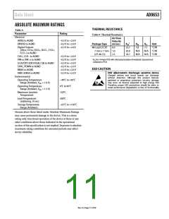
ABSOLUTE MAXIMUM RATINGS
THERMAL RESISTANCE
Table 8.
Parameter
Rating
Table 9. Thermal Resistance
Electrical
Air Flow
Velocity
(m/sec)
AVDD to AGND
DRVDD to AGND
Digital Outputs
−0.3 V to +2.0 V
−0.3 V to +2.0 V
−0.3 V to +2.0 V
1
Package Type
θJA
θJB
θJC
7.1
Unit
48-Lead LFCSP
0.0
23.7
20.0
18.7
7.8
N/A
N/A
°C/W
(D0 x, D1 x, DCO+, DCO−, FCO+,
7 mm × 7 mm 1.0
(CP-48-13) 2.5
N/A °C/W
N/A °C/W
FCO−) to AGND
CLK+, CLK− to AGND
VIN+x, VIN−x to AGND
SCLK/DTP, SDIO/OLM, CSB to AGND
SYNC, PDWN to AGND
RBIAS to AGND
−0.3 V to +2.0 V
−0.3 V to +2.0 V
−0.3 V to +2.0 V
−0.3 V to +2.0 V
−0.3 V to +2.0 V
−0.3 V to +2.0 V
1 θJA for a 4-layer PCB with solid ground plane (simulated). Exposed pad
soldered to PCB.
ESD CAUTION
VREF, SENSE to AGND
Environmental
Operating Temperature
Range (Ambient, VREF = 1.0 V)
Operating Temperature
Range (Ambient, VREF = 1.3 V)
Maximum Junction
Temperature
−40°C to +85°C
0°C to 85°C
150°C
Lead Temperature
(Soldering, 10 sec)
300°C
Storage Temperature
Range (Ambient)
−65°C to +150°C
Stresses above those listed under Absolute Maximum Ratings
may cause permanent damage to the device. This is a stress
rating only; functional operation of the device at these or any
other conditions above those indicated in the operational
section of this specification is not implied. Exposure to absolute
maximum rating conditions for extended periods may affect
device reliability.
Rev. 0 | Page 11 of 40

 ADI [ ADI ]