AD9653
Data Sheet
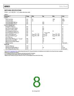
SWITCHING SPECIFICATIONS
AVDD = 1.8 V, DRVDD = 1.8 V, unless otherwise noted.
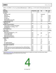
Table 6.
Parameter1, 2
Temp
Min
Typ
Max
Unit
CLOCK3
Input Clock Rate
Conversion Rate
Full
Full
Full
Full
20
20
1000
125
MHz
MSPS
ns
Clock Pulse Width High (tEH)
Clock Pulse Width Low (tEL)
OUTPUT PARAMETERS3
Propagation Delay (tPD)
Rise Time (tR) (20% to 80%)
Fall Time (tF) (20% to 80%)
FCO Propagation Delay (tFCO
DCO Propagation Delay (tCPD
DCO to Data Delay (tDATA
DCO to FCO Delay (tFRAME
Lane Delay (tLD)
4.00
4.00
ns
Full
Full
Full
Full
Full
Full
Full
2.3
300
300
2.3
ns
ps
ps
ns
ns
ps
ps
ps
)
)
1.5
3.1
4
tFCO + (tSAMPLE/16)
(tSAMPLE/16)
(tSAMPLE/16)
90
4
)
(tSAMPLE/16) − 300
(tSAMPLE/16) − 300
(tSAMPLE/16) + 300
(tSAMPLE/16) + 300
4
)
Data to Data Skew (tDATA-MAX − tDATA-MIN
Wake-Up Time (Standby)
Wake-Up Time (Power-Down)5
Pipeline Latency
)
Full
50
200
ps
ns
μs
25°C
25°C
Full
250
375
16
Clock cycles
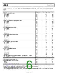
APERTURE
Aperture Delay (tA)
Aperture Uncertainty (Jitter, tJ)
Out-of-Range Recovery Time
25°C
25°C
25°C
1
135
1
ns
fs rms
Clock cycles
1 See the AN-835 Application Note, Understanding High Speed ADC Testing and Evaluation, for definitions and for details on how these tests were completed.
2 Measured on standard FR-4 material.
3 Can be adjusted via the SPI. The conversion rate is the clock rate after the divider.
4 tSAMPLE/16 is based on the number of bits in two LVDS data lanes. tSAMPLE = 1/fS.
5 Wake-up time is defined as the time required to return to normal operation from power-down mode.
Rev. 0 | Page 8 of 40

 ADI [ ADI ]