AD8132
LAYOUT, GROUNDING, AND BYPASSING
As a high speed part, the AD8132 is sensitive to the PCB envi-
ronment in which it operates. Realizing its superior specifications
requires attention to various details of good high speed PCB design.
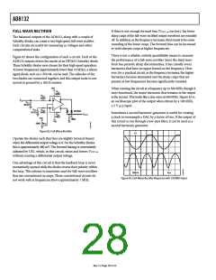
CIRCUITS
R
F1
R
R
G1
+
The first requirement is a good solid ground plane that covers as
much of the board area around the AD8132 as possible. The only
exception to this is that the two input pins (Pin 1 and Pin 8) are
kept a few millimeters from the ground plane and that ground
be removed from inner layers and the opposite side of the board
under the input pins. This minimizes the stray capacitance on
these nodes and helps preserve the gain flatness vs. the frequency.
G2
R
F2
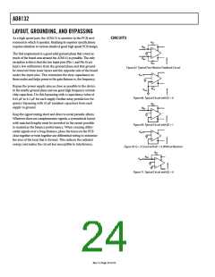
Figure 67. Typical Four-Resistor Feedback Circuit
V
+
IN
Bypass the power supply pins as close as possible to the device
to the nearby ground plane and use good high frequency ceramic
chip capacitors. Do this bypassing with a capacitance value of
0.01 μF to 0.1 μF for each supply. Farther away, provide low fre-
quency bypassing with 10 μF tantalum capacitors from each
supply to ground.
R
F2
R
G2
Figure 68. Typical Circuit with β1 = 0
R
F1
R
G1
+
Keep the signal routing short and direct to avoid parasitic effects.
Wherever there are complementary signals, a symmetrical layout
with matched lengths must be provided to the extent possible
to maximize the balance performance. When running differ-
ential signals over a long distance, place the traces on the PCB
close together or twist together any differential wiring to minimize
the area of the loop that is formed. This reduces the radiated
energy and makes the circuit less susceptible to interference.
Figure 69. Typical Circuit with β2 = 1
V
+
IN
Figure 70. G = 2 Circuit with β1 = 0, Without Resistors
R
F1
R
G1
V
IN
+
Figure 71. Typical Circuit with β2 = 0
Rev. F | Page 24 of 32

 ADI [ ADI ]