AD8132
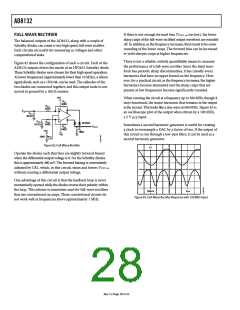
If there is not enough forward bias (VOUT, cm too low), the lower
sharp cusps of the full-wave rectified output waveform are rounded
off. In addition, as the frequency increases, there tends to be some
rounding of the lower cusps. The forward bias can be increased
to yield sharper cusps at higher frequencies.
FULL-WAVE RECTIFIER
The balanced outputs of the AD8132, along with a couple of
Schottky diodes, can create a very high speed, full-wave rectifier.
Such circuits are useful for measuring ac voltages and other
computational tasks.
There is not a reliable, entirely quantifiable means to measure
the performance of a full-wave rectifier. Since the ideal wave-
form has periodic sharp discontinuities, it has (mostly even)
harmonics that have no upper bound on the frequency. How-
ever, for a practical circuit, as the frequency increases, the higher
harmonics become attenuated and the sharp cusps that are
present at low frequencies become significantly rounded.
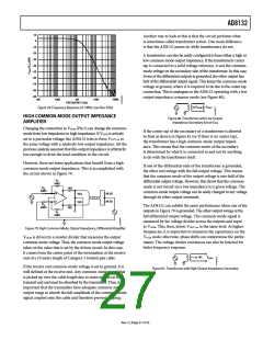
Figure 82 shows the configuration of such a circuit. Each of the
AD8132 outputs drives the anode of an HP2835 Schottky diode.
These Schottky diodes were chosen for their high speed operation.
At lower frequencies (approximately lower than 10 MHz), a silicon
signal diode, such as a 1N4148, can be used. The cathodes of the
two diodes are connected together, and this output node is con-
nected to ground by a 100 Ω resistor.
+5V
When running the circuit at a frequency up to 300 MHz, though it
stays functional, the major harmonic that remains in the output
is the second. This looks like a sine wave at 600 MHz. Figure 83 is
an oscilloscope plot of the output when driven by a 100 MHz,
2.5 V p-p input.
R
348Ω
F1
R
G1
348Ω
V
IN
R
T1
49.9Ω
R
24.9Ω
R
348Ω
T2
G2
HP2835
Sometimes a second harmonic generator is useful for creating
a clock to oversample a DAC by a factor of two. If the output of
this circuit is run through a low-pass filter, it can be used as a
second harmonic generator.
R
V
OUT
F2
R
100Ω
348Ω
L
+5V
10kΩ
–5V
CR1
Figure 82. Full-Wave Rectifier
1V
Operate the diodes such that they are slightly forward-biased
when the differential output voltage is 0. For the Schottky diodes,
this is approximately 400 mV. The forward biasing is conveniently
adjusted by CR1, which, in this circuit, raises and lowers VOUT, cm
without creating a differential output voltage.
One advantage of this circuit is that the feedback loop is never
momentarily opened while the diodes reverse their polarity within
the loop. This scheme is sometimes used for full-wave rectifiers
that use conventional op amps. These conventional circuits do
not work well at frequencies above approximately 1 MHz.
100mV
2ns
Figure 83. Full-Wave Rectifier Response with 100 MHz Input
Rev. F | Page 28 of 32

 ADI [ ADI ]