AD8132
OPERATIONAL DESCRIPTION
Table 10. Differential and Common-Mode Gains
DEFINITION OF TERMS
Input
VIN, dm
VIN, cm
VOCM
VOUT, dm
VOUT, cm
Differential Voltage
RF/RG
0
0
0 (by design)
0 (by design)
1 (by design)
The difference between two node voltages. For example, the
output differential voltage (or equivalently output differential-
mode voltage) is defined as
As listed in Table 10, the differential output (VOUT, dm) is equal to
the differential input voltage (VIN, dm) times RF/RG. In this case,
it does not matter if both differential inputs are driven, or only
one output is driven and the other is tied to a reference voltage,
such as ground. As seen from the two zero entries in the VOUT, dm
column, neither of the common-mode inputs has any effect on
this gain.
V
OUT, dm = (V+OUT − V−OUT)
where V+OUT and V−OUT refer to the voltages at the +OUT and
−OUT terminals with respect to a common reference.
Common-Mode Voltage
The average of two node voltages. The output common-mode
voltage is defined as
V
OUT, cm = (V+OUT + V−OUT)/2
The gain from VIN, dm to VOUT, cm is 0, and first-order does not
depend on the ratio matching of the feedback networks. The
common-mode feedback loop within the AD8132 provides a cor-
rective action to keep this gain term minimized. The term balance
error describes the degree that this gain term differs from 0.
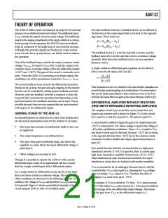
C
F
R
F
R
R
G
G
+IN
–IN
–OUT
+OUT
+D
IN
The gain from VIN, cm to VOUT, dm directly depends on the matching
of the feedback networks. The analogous term for this transfer
function (used in conventional op amps) is common-mode reject-
tion ratio (CMRR). Therefore, if it has a high CMRR, the feedback
ratios must be well matched.
R
V
O, dm
V
AD8132
L, dm
OCM
–D
IN
R
F
C
F
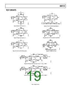
Figure 64. Circuit Definitions
The gain from VIN, cm to VOUT, cm is ideally 0 and is first-order
independent of the feedback ratio matching. As in the case of
VIN, dm to VOUT, cm, the common-mode feedback loop keeps this
term minimized.
BASIC CIRCUIT OPERATION
One of the more useful and easy to understand ways to use
the AD8132 is to provide two equal-ratio feedback networks.
To match the effect of parasitics, comprise these networks of
two equal-value feedback resistors (RF) and two equal-value
gain resistors (RG). This circuit is shown in Figure 64.
The gain from VOCM to VOUT, dm is ideally 0 when the feedback ratios
are matched only. The amount of differential output signal that is
created by varying VOCM is related to the degree of mismatch in the
feedback networks.
Like a conventional op amp, the AD8132 has two differential
inputs that can be driven with both differential-mode input
voltage (VIN, dm) and common-mode input voltage (VIN, cm).
VOCM controls the output common-mode voltage VOUT, cm with
a unity-gain transfer function. With equal-ratio feedback net-
works (as previously assumed), its effect on each output is the
same, that is the gain from VOCM to VOUT, dm is 0. If not driven,
the output common-mode voltage is set with an internal voltage
divider to a level that is nominally midsupply. It is recommended
There is another input (VOCM) that is not present on conventional
op amps, but provides another input to consider on the AD8132.
It is totally separate from the previous inputs.
There are two complementary outputs whose response can be
defined by a differential-mode output (VOUT, dm) and a common-
mode output (VOUT, cm).
that a 0.1 μF bypass capacitor be connected to VOCM
.
When unequal feedback ratios are used, the two gains associated
with VOUT, dm become nonzero. This significantly complicates
the mathematical analysis along with any intuitive understanding
of how the part operates.
Table 10 indicates the gain from any type of input to either type
of output.
Rev. F | Page 20 of 32

 ADI [ ADI ]