AD8132
+5V
+5V
+
0.1µF
1kΩ
10µF
+
0.1µF
10µF
499Ω
49.9Ω
1
49.9Ω
50Ω
SOURCE
100Ω
AD8132
0.1µF
523Ω
2
3
AD830
TWISTED
PAIR
7
49.9Ω
V
OUT
4
1kΩ
0.1µF
–5V
10µF
5
+
10µF
0.1µF
–5V
+
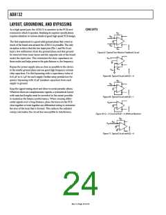
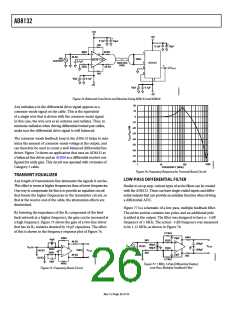
Figure 74. Balanced Line Driver and Receiver Using AD8132 and AD830
20
Any imbalance in the differential drive signal appears as a
common-mode signal on the cable. This is the equivalent
of a single wire that is driven with the common-mode signal.
In this case, the wire acts as an antenna and radiates. Thus, to
minimize radiation when driving differential twisted pair cables,
make sure the differential drive signal is well balanced.
10
0
–10
–20
–30
–40
–50
–60
–70
–80
The common-mode feedback loop in the AD8132 helps to min-
imize the amount of common-mode voltage at the output, and
can therefore be used to create a well-balanced differential line
driver. Figure 74 shows an application that uses an AD8132 as
a balanced line driver and an AD830 as a differential receiver con-
figured for unity gain. This circuit was operated with 10 meters of
Category 5 cable.
1000
1
10
100
FREQUENCY (MHz)
Figure 76. Frequency Response for Transmit Boost Circuit
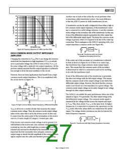
TRANSMIT EQUALIZER
LOW-PASS DIFFERENTIAL FILTER
Any length of transmission line attenuates the signals it carries.
This effect is worse at higher frequencies than at lower frequencies.
One way to compensate for this is to provide an equalizer circuit
that boosts the higher frequencies in the transmitter circuit, so
that at the receive end of the cable, the attenuation effects are
diminished.
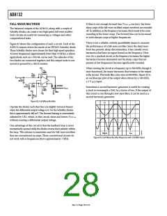
Similar to an op amp, various types of active filters can be created
with the AD8132. These can have single-ended inputs and differ-
ential outputs that can provide an antialias function when driving
a differential ADC.
Figure 77 is a schematic of a low-pass, multiple feedback filter.
The active section contains two poles, and an additional pole
is added at the output. The filter was designed to have a −3 dB
frequency of 1 MHz. The actual −3 dB frequency was measured
to be 1.12 MHz, as shown in Figure 78.
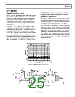
By lowering the impedance of the RG component of the feed-
back network at a higher frequency, the gain can be increased at
a high frequency. Figure 75 shows the gain of a two-line driver
that has its RG resistors shunted by 10 pF capacitors. The effect
of this is shown in the frequency response plot of Figure 76.
2.15kΩ
549Ω
499Ω
33pF
10pF
2kΩ
100pF
100pF
2kΩ
953Ω
953Ω
49.9Ω
200pF
200pF
V
V
49.9Ω
IN
OUT
V
IN
249Ω
249Ω
100Ω
49.9Ω
V
OUT
49.9Ω
24.9Ω
33pF
24.9Ω
54Ω
2.15kΩ
10pF
499Ω
Figure 77. 1 MHz, 3-Pole Differential Output,
Low-Pass, Multiple Feedback Filter
Figure 75. Frequency Boost Circuit
Rev. F | Page 26 of 32

 ADI [ ADI ]