AD8132
APPLICATIONS
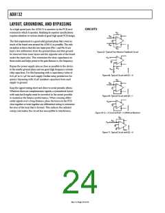
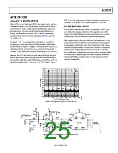
FFT plot of the performance of the circuit when running at a
clock rate of 40 MSPS and an input frequency of 2.5 MHz.
ANALOG-TO-DIGITAL DRIVER
Many of the newer high speed ADCs are single-supply and have
differential inputs. Thus, the driver for these devices is able to
convert from a single-ended signal to a differential signal and
provide output common-mode level shifting in addition to
having low distortion and noise. The AD8132 conveniently
performs these functions when driving the AD9203, a 10-bit,
40 MSPS ADC.
BALANCED CABLE DRIVER
When driving a twisted pair cable, it is desirable to drive only a
pure differential signal onto the line. If the signal is purely differ-
ential (that is, fully balanced), and the transmission line is twisted
and balanced, there is minimum radiation of any signal.
The complementary electrical fields are confined mostly to the
space between the two twisted conductors and does not signif-
icantly radiate out from the cable. The current in the cable creates
magnetic fields that radiate to some degree. However, the amount
of radiation is mitigated by the twists, because for each twist,
the two adjacent twists have an opposite polarity magnetic field.
If the twist pitch is tight enough, these small magnetic field loops
contain most of the magnetic flux, and the magnetic farfield
strength is negligible.
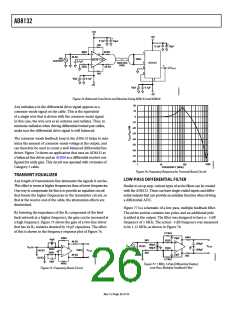
In Figure 73, a 1 V p-p signal drives the input of an AD8132
configured for unity gain. Both the AD8132 and the AD9203 are
powered from a single 3 V supply. A voltage divider biases VOCM
at midsupply and in turn drives VOUT, cm to half of the supply
voltage. This is within the common-mode range of the AD9203.
Between the ADC and the driver is a 1-pole, differential filter that
helps to filter some of the noise and assists the switched-capacitor
inputs of the ADC. Each of the ADC inputs is driven by a 0.5 V p-p
signal that ranges from 1.25 V dc to 1.75 V dc. Figure 72 is an
10
f
f
= 40MHz
= 2.5MHz
FUND
S
0
IN
–10
–20
–30
–40
–50
–60
–70
–80
2ND
5TH
12.5
6TH
8TH
9TH
7TH
3RD
4TH
–90
–100
–110
–120
0
2.5
5.0
7.5
10.0
15.0
17.5
20.0
INPUT FREQUENCY (MHz)
Figure 72. FTT Response for AD8132 Driving AD9203
3V
10kΩ
3V
3V
+
0.1µF
10µF
348Ω
0.1µF
10kΩ
348Ω
0.1µF
1V p-p
28
2
60.4Ω
AVDD
DRVDD
25
3
8
2
AINN
5
20pF
20pF
49.9Ω
DIGITAL
OUTPUTS
AD9203
AD8132
0.1µF
4
AINP
26
348Ω
24.9Ω
60.4Ω
1
6
AVSS
27
DRVSS
1
348Ω
Figure 73. AD8132 Driving AD9203, a 10-Bit, 40 MSPS ADC
Rev. F | Page 25 of 32

 ADI [ ADI ]