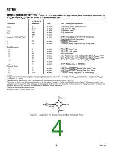
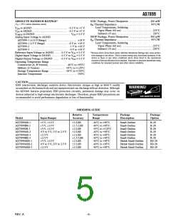
AD7899
CONVERTER DETAILS
external CONVST signal and the track/hold actually going into
hold) is typically 15 ns and, more importantly, is well matched
from device to device. It allows multiple AD7899s to sample
more than one channel simultaneously. At the end of a conversion,
the part returns to its tracking mode. The acquisition time of
the track/hold amplifier begins at this point.
The AD7899 is a high-speed, low-power, 14-bit A/D converter
that operates from a single 5 V supply. The part contains a
2.2 µs successive-approximation ADC, track/hold amplifier, an
internal 2.5 V reference and a high-speed parallel interface. The
part accepts an analog input range of 10 V or 5 V (AD7899-1),
0 V to 2.5 V or 0 V to 5 V (AD7899-2) and 2.5 V (AD7899-3).
Overvoltage protection on the analog inputs for the part allows
the input voltage to go to 18 V (AD7899-1 with 10 V input
range), –9 V to +18 V (AD7899-1 with 5 V input range), –1 V
to +18 V (AD7899-2) and –4 V to +18 V (AD7899-3) without
causing damage.
Reference Section
The AD7899 contains a single reference pin, labelled VREF
,
which either provides access to the part’s own 2.5 V reference or
allows an external 2.5 V reference to be connected to provide
the reference source for the part. The part is specified with a
2.5 V reference voltage.
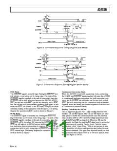
A conversion is initiated on the AD7899 by pulsing the CONVST
input. On the rising edge of CONVST, the on-chip track/hold is
placed into hold and the conversion is started. The BUSY/EOC
output signal is triggered high on the rising edge of CONVST
and will remain high for the duration of the conversion sequence.
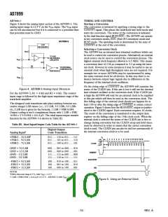
The conversion clock for the part is generated internally using a
laser-trimmed clock oscillator circuit. There is also the option of
using an external clock. An external noncontinuous clock is applied
to the CLKIN pin. If, on the rising edge of CONVST, this input
is high, the external clock will be used. The external clock should
not start until 100 ns after the rising edge of CONVST. The
optimum throughput is obtained by using the internally gener-
ated clock—see Using an External Clock. The BUSY/EOC signal
indicates the end of the conversion, and at this time the Track and
Hold returns to tracking mode. The conversion results can be
read at the end of the conversion (indicated by BUSY/EOC
going low) via a 14-bit parallel data bus with standard CS and RD
signals—see Timing and Control.
To use the internal reference as the reference source for the
AD7899, simply connect a 0.1 µF capacitor from the VREF pin
to AGND. The voltage that appears at this pin is internally
buffered before being applied to the ADC. If this reference is
required for use external to the AD7899, it should be buffered,
as the part has a FET switch in series with the reference output
resulting in a source impedance for this output of 6 kΩ nominal.
The tolerance on the internal reference is 10 mV at 25°C with
a typical temperature coefficient of 25 ppm/°C and a maximum
error over temperature of 20 mV.
If the application requires a reference with a tighter tolerance or
the AD7899 needs to be used with a system reference, the user
has the option of connecting an external reference to this VREF
pin. The external reference will effectively overdrive the internal
reference and thus provide the reference source for the ADC.
The reference input is buffered before being applied to the ADC
with the maximum input current of 100 µA. Suitable reference
sources for the AD7899 include the AD680, AD780, REF192,
and REF43 precision 2.5 V references.
Conversion time for the AD7899 is 2.2 µs and the track/hold
acquisition time is 0.3 µs. To obtain optimum performance from
the part, the read operation should not occur during a conversion
or during the 150 ns prior to the next CONVST rising edge.
This allows the part to operate at throughput rates up to 400 kHz
and achieve data sheet specifications.
Analog Input Section
The AD7899 is offered as three part types, the AD7899-1 where
the input can be configured for 10 V or a 5 V input voltage
range, the AD7899-2 where the input can be configured for 0 V
to 5 V or a 0 V to 2.5 V input voltage range and the AD7899-3
which handles input voltage range 2.5 V. The amount of current
flowing into the analog input will depend on the analog input
range and the analog input voltage. The maximum current flows
when negative full-scale is applied.
CIRCUIT DESCRIPTION
Track/Hold Section
The track/hold amplifier on the AD7899 allows the ADCs to
accurately convert an input sine wave of full-scale amplitude to
14-bit accuracy. The input bandwidth of the track/hold is greater
than the Nyquist rate of the ADC even when the ADC is oper-
ated at its maximum throughput rate of 400 kSPS (i.e., the
track/hold can handle input frequencies in excess of 200 kHz).
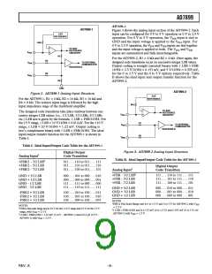
AD7899-1
Figure 2 shows the analog input section of the AD7899-1. The
input can be configured for 5 V or 10 V operation on the
AD7899-1. For 5 V operation, the VINA and VINB inputs are
tied together and the input voltage is applied to both. For 10 V
operation, the VINB input is tied to AGND and the input voltage
is applied to the VINA input. The VINA and VINB inputs are sym-
metrical and fully interchangeable.
The track/hold amplifier’s acquire input signals to 14-bit
accuracy in less than 300 ns The operation of the track/hold is
essentially transparent to the user. The track/hold amplifier
samples the input channel on the rising edge of CONVST. The
aperture time for the track/hold (i.e., the delay time between the
–8–
REV. A

 ADI [ ADI ]