AD7899
AD7899-3
TIMING AND CONTROL
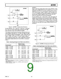
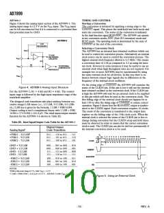
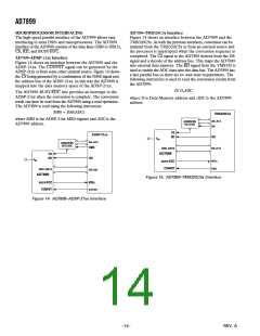
Figure 4 shows the analog input section of the AD7899-3. The
analog input range is 2.5 V on the VINA input. The VINB input
can be left unconnected but if it is connected to a potential then
that potential must be GND.
Starting a Conversion
The conversion is initiated by applying a rising edge to the
CONVST signal. This places the track/hold into hold mode and
starts the conversion. The status of the conversion is indicated
by the dual function signal BUSY/EOC. The AD7899 can operate
in two conversion modes, EOC (End Of Conversion) mode and
BUSY mode. The operating mode is determined by the state of
CONVST at the end of the conversion.
AD7899-3
2.5V
REFERENCE
Selecting a Conversion Clock
6k⍀
The AD7899 has an internal laser trimmed oscillator which can
be used to control the conversion process. Alternatively an external
clock source can be used to control the conversion process. The
highest external clock frequency allowed is 6.5 MHz. This means
a conversion time of 2.46 µs compared to 2.2 µs using the inter-
nal clock. However in some instances it may be useful to use an
external clock when high throughput rates are not required. For
example two or more AD7899s may be synchronized by using
the same external clock for all devices. In this way there is no
latency between output logic signals due to differences in the
frequency of the internal clock oscillators.
TO ADC
REFERENCE
V
REF
CIRCUITRY
R1
R2
TO INTERNAL
COMPARATOR
V
INA
TRACK/HOLD
V
INB
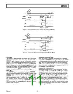
On the rising edge of CONVST the AD7899 will examine the
status of the CLKIN pin. If this pin is low it will use the internal
laser trimmed oscillator as the conversion clock. If the CLKIN pin
is high the AD7899 will wait for an external clock to be supplied
to this pin which will then be used as the conversion clock. The
first falling edge of the external clock should not happen for at
least 100 ns after the rising edge of CONVST to ensure correct
operation. Figure 5 shows how the BUSY/EOC output is synchro-
nized to the CLKIN signal. Each conversion requires 16 clocks.
The result of the conversion is transferred to the output data
register on the falling edge of the 15th clock cycle. When the
internal clock is selected the status of the CLKIN pin is free to
change during conversion but the CLKIN setup and hold times
must be observed in order to ensure that the correct conversion
clock is used. The CLKIN pin can also be tied low permanently if
the internal conversion clock is to be used.
Figure 4. AD7899-3 Analog Input Structure
For the AD7899-3, R1 = 4 kΩ and R2 = 4 kΩ. The resistor
input stage is followed by the high input impedance stage of the
track/hold amplifier.
The designed code transitions take place midway between suc-
cessive integer LSB values (i.e., 1/2 LSB, 3/2 LSBs, 5/2 LSBs
etc.) LSB size is given by the formula, 1 LSB = FSR/16384.
Output coding is two’s complement binary with 1 LSB = FSR/
16384 = 5 V/16384 = 610.4 µV. The ideal input/output transfer
function for the AD7899-3 is shown in Table III.
Table III. Ideal Input/Output Code Table for the AD7899-3
Digital Output
Analog Inputl
Code Transition
+FSR/2 – 3/2 LSB2
+FSR/2 – 5/2 LSB
+FSR/2 – 7/2 LSB
011 . . . 110 to 011 . . . 111
011 . . . 101 to 011 . . . 110
011 . . . 100 to 011 . . . 101
t9
1
2 3 4 5 6 7 8 9 10 11 12 13 14 15 16
CLKIN
t11
GND + 3/2 LSB
GND + 1/2 LSB
GND – 1/2 LSB
GND – 3/2 LSB
000 . . . 001 to 000 . . . 010
000 . . . 000 to 000 . . . 001
111 . . . 111 to 000 . . . 000
111 . . . 110 to 111 . . . 111
CONVST
BUSY/EOC
–FSR/2 + 5/2 LSB
–FSR/2 + 3/2 LSB
–FSR/2 + 1/2 LSB
100 . . . 010 to 100 . . . 011
100 . . . 001 to 100 . . . 010
100 . . . 000 to 100 . . . 001
RD
CS
NOTES
1FSR is full-scale range is 5 V, with VREF = 2.5 V
21 LSB = FSR/16384 = 610.4 µV ( 2.5 V – AD7899-3) with VREF = 2.5 V.
Figure 5. Using an External Clock
–10–
REV. A

 ADI [ ADI ]