AD7899
AD7899-2
AD7899-1
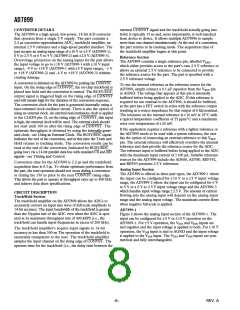
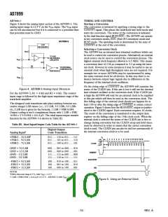
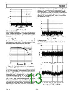
Figure 3 shows the analog input section of the AD7899-2. Each
input can be configured for 0 V to 5 V operation or 0 V to 2.5 V
operation. For 0 V to 5 V operation, the VINB input is tied to
GND and the input voltage is applied to the VINA input. For
0 V to 2.5 V operation, the VINA and VINB inputs are tied together
and the input voltage is applied to both. The VINA and VINB
inputs are symmetrical and fully interchangeable.
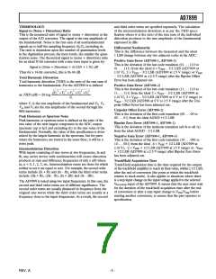
2.5V
REFERENCE
6k⍀
TO ADC
REFERENCE
CIRCUITRY
V
REF
R1
For the AD7899-2, R1 = 4 kΩ and R2 = 4 kΩ. Once again, the
designed code transitions occur on successive integer LSB values.
Output coding is straight (natural) binary with 1 LSB = FSR/
16384 = 2.5 V/16384 = 0.153 mV, and 5 V/16384 = 0.305 mV,
for the 0 to 2.5 V and the 0 to 5 V options respectively. Table
II shows the ideal input and output transfer function for the
AD7899-2.
R2
R3
TO INTERNAL
COMPARATOR
TRACK/HOLD
V
INA
V
INB
R4
GND
AD7899-2
Figure 2. AD7899-1 Analog Input Structure
2.5V
REFERENCE
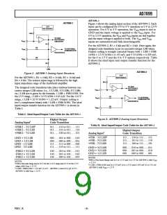
For the AD7899-1, R1 = 4 kΩ, R2 = 16 kΩ, R3 = 16 kΩ and
R4 = 8 kΩ. The resistor input stage is followed by the high
input impedance stage of the track/hold amplifier.
6k⍀
TO ADC
The designed code transitions take place midway between suc-
cessive integer LSB values (i.e., 1/2 LSB, 3/2 LSBs, 5/2 LSBs
etc.) LSB size is given by the formula, 1 LSB = FSR/16384. For
the 5 V range, 1 LSB = 10 V/16384 = 610.4 µV. For the 10 V
range, 1 LSB = 20 V/16384 = 1.22 mV. Output coding is
two’s complement binary with 1 LSB = FSR/16384. The ideal
input/output transfer function for the AD7899-1 is shown in
Table I.
REFERENCE
V
REF
CIRCUITRY
R1
R2
TO INTERNAL
COMPARATOR
V
INA
TRACK/HOLD
V
INB
Table I. Ideal Input/Output Code Table for the AD7899-1
Digital Output
Figure 3. AD7899-2 Analog Input Structure
Analog Input1
Code Transition
Table II. Ideal Input/Output Code Table for the AD7899-2
Digital Output
+FSR/2 – 3/2 LSB2
+FSR/2 – 5/2 LSB
+FSR/2 – 7/2 LSB
011 . . . 110 to 011 . . . 111
011 . . . 101 to 011 . . . 110
011 . . . 100 to 011 . . . 101
Analog Input1
Code Transition
+FSR – 3/2 LSB2
+FSR – 5/2 LSB
+FSR – 7/2 LSB
111 . . . 110 to 111 . . . 111
111 . . . 101 to 111 . . . 110
111 . . . 100 to 111 . . . 101
GND + 3/2 LSB
GND + 1/2 LSB
GND – 1/2 LSB
GND – 3/2 LSB
000 . . . 001 to 000 . . . 010
000 . . . 000 to 000 . . . 001
111 . . . 111 to 000 . . . 000
111 . . . 110 to 111 . . . 111
GND + 5/2 LSB
GND + 3/2 LSB
GND + 1/2 LSB
000 . . . 010 to 000 . . . 011
000 . . . 001 to 000 . . . 010
000 . . . 000 to 000 . . . 001
–FSR/2 + 5/2 LSB
–FSR/2 + 3/2 LSB
–FSR/2 + 1/2 LSB
100 . . . 010 to 100 . . . 011
100 . . . 001 to 100 . . . 010
100 . . . 000 to 100 . . . 001
NOTES
1FSR is Full-Scale Range and is 0 to 2.5 V and 0 to 5 V for AD7899-2 with VREF
= 2.5 V.
NOTES
1FSR is full-scale range and is 20 V for the 10 V range and 10 V for the 5 V
range, with VREF = 2.5 V.
21 LSB = FSR/16384 and is 0.153 mV (0 to 2.5 V) and 0.305 mV (0 to 5 V) for
AD7899-2 with VREF = 2.5 V.
21 LSB = FSR/16384 = 1.22 mV ( 10 V – AD7899-1) and 610.4 µV ( 5 V –
AD7899-1) with VREF = 2.5 V.
–9–
REV. A

 ADI [ ADI ]