AD7899
TIMING CHARACTERISTICS1, 2
(VDD = 5 V ؎ 5%, AGND = DGND = 0 V, VREF = Internal, Clock = Internal; All specifications TMIN
to TMAX and valid for VDRIVE = 3 V ؎ 5% and 5 V ؎ 5% unless otherwise noted.)
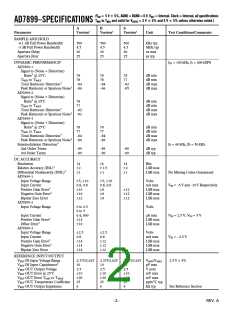
A, B and S
Versions
Parameter
Unit
Test Conditions/Comments
tCONV
2.2
2.46
0.3
120
180
2
µs max
µs max
µs max
ns min
ns max
µs max
Conversion Time, Internal Clock
CLKIN = 6.5 MHz
Acquisition Time
tACQ
tEOC
EOC Pulsewidth
5
tWAKE-UP – External VREF
STBY Rising Edge to CONVST Rising Edge
(See Standby Mode Operation)
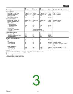
t1
t2
35
70
ns min
ns min
CONVST Pulsewidth
CONVST Rising Edge to BUSY Rising Edge
Read Operation
t3
t4
0
0
ns min
ns min
ns min
ns max
ns max
ns min
ns max
ns min
CS to RD Setup Time
CS to RD Hold Time
Read Pulsewidth
Data Access Time after Falling Edge of RD, VDRIVE = 5 V
Data Access Time after Falling Edge of RD, VDRIVE = 3 V
Bus Relinquish Time after Rising Edge of RD
t53
35
35
40
5
30
0
t6
4
t7
t8
BUSY Falling Edge to RD Delay
External Clock
t9
t10
t11
0
20
100
ns min
ns min
ns min
CLKIN to CONVST Rising Edge Setup Time
CLKIN to CONVST Rising Edge Hold Time
CONVST Rising Edge to CLK Falling Edge
NOTES
1 Sample tested at 25°C to ensure compliance. All input signals are measured with tr = tf = 1 ns (10% to 90% of VDRIVE) and timed from a voltage level of VDRIVE/2.
2 See Figures 5, 6, 7, and 8.
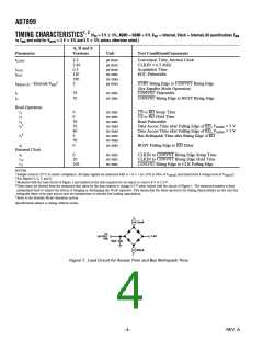
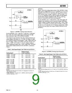
3 Measured with the load circuit of Figure 1 and defined as the time required for an output to cross 0.8 V or 2.0 V.
4These times are derived from the measured time taken by the data outputs to change 0.5 V when loaded with the circuit of Figure 1. The measured number is then
extrapolated back to remove the effects of charging or discharging the 50 pF capacitor. This means that the times quoted in the timing characteristics are the true bus
relinquish times of the part and as such are independent of external bus loading capacitances.
5 Refer to the Standby Mode Operation section.
Specifications subject to change without notice.
1.6mA
TO
OUTPUT
PIN
1.6V
50pF
400A
Figure 1. Load Circuit for Access Time and Bus Relinquish Time
–4–
REV. A

 ADI [ ADI ]