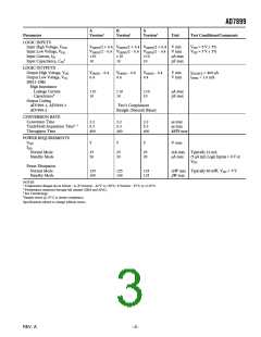
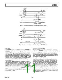
AD7899
TERMINOLOGY
Signal to (Noise + Distortion) Ratio
and third order terms are specified separately. The calculation
of the intermodulation distortion is as per the THD speci-
fication where it is the ratio of the rms sum of the individual
distortion products to the rms amplitude of the fundamental
expressed in dBs.
This is the measured ratio of signal to (noise + distortion) at the
output of the A/D converter. The signal is the rms amplitude of
the fundamental. Noise is the rms sum of all nonfundamental
signals up to half the sampling frequency (fS/2), excluding dc.
The ratio is dependent upon the number of quantization levels
in the digitization process; the more levels, the smaller the quan-
tization noise. The theoretical signal to (noise + distortion) ratio
for an ideal N-bit converter with a sine wave input is given by:
Differential Nonlinearity
This is the difference between the measured and the ideal
1 LSB change between any two adjacent codes in the ADC.
Positive Gain Error (AD7899-1, AD7899-3)
This is the deviation of the last code transition (01 . . . 110 to
01 . . . 111) from the ideal 4 × VREF – 3/2 LSB (AD7899 at
10 V), 2 × VREF – 3/2 LSB (AD7899 at 5 V range) or VREF
– 3/2 LSB (AD7899 at 2.5 V range) after the Bipolar Offset
Error has been adjusted out.
Signal to (Noise + Distortion) = (6.02N + 1.76) dB
Thus for a 14-bit converter, this is 86.04 dB.
Total Harmonic Distortion
Total harmonic distortion (THD) is the ratio of the rms sum of
harmonics to the fundamental. For the AD7899 it is defined
Positive Gain Error (AD7899-2)
This is the deviation of the last code transition (11 . . . 110 to
11 . . . 111) from the ideal 2 × VREF – 3/2 LSB (AD7899 at
10 V), 2 × VREF – 3/2 LSB (AD7899 at 0 V to 5 V range) or
VREF – 3/2 LSB (AD7899 at 0 V to 2.5 V range) after the Uni-
polar Offset Error has been adjusted out.
2
V22 +V32 +V4 +V52 +V62
as:THD (dB) = 20 log
V
1
where V1 is the rms amplitude of the fundamental and V2, V3,
V4, and V5 are the rms amplitudes of the second through the
fifth harmonics.
Unipolar Offset Error (AD7899-2)
This is the deviation of the first code transition (00 . . . 00 to
00 . . . 01) from the ideal AGND +1/2 LSB
Peak Harmonic or Spurious Noise
Peak harmonic or spurious noise is defined as the ratio of the
rms value of the next largest component in the ADC output
spectrum (up to fS/2 and excluding dc) to the rms value of the
fundamental. Normally, the value of this specification is deter-
mined by the largest harmonic in the spectrum, but for parts
where the harmonics are buried in the noise floor, it will be a
noise peak.
Bipolar Zero Error (AD7899-1, AD7899-2)
This is the deviation of the midscale transition (all 0s to all 1s)
from the ideal AGND – 1/2 LSB.
Negative Gain Error (AD7899-1, AD7899-3)
This is the deviation of the first code transition (10 . . . 000 to
10 . . . 001) from the ideal –4 × VREF + 1/2 LSB (AD7899 at
10 V), –2 × VREF + 1/2 LSB (AD7899 at 5 V range) or –VREF
+ 1/2 LSB (AD7899 at 2.5 V range) after Bipolar Zero Error
has been adjusted out.
Intermodulation Distortion
With inputs consisting of sine waves at two frequencies, fa and
fb, any active device with nonlinearities will create distortion
products at sum and difference frequencies of mfa nfb where
m, n = 0, 1, 2, 3, etc. Intermodulation terms are those for which
neither m nor n are equal to zero. For example, the second order
terms include (fa + fb) and (fa – fb), while the third order terms
include (2fa + fb), (2fa – fb), (fa + 2fb) and (fa – 2fb).
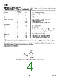
Track/Hold Acquisition Time
Track/Hold acquisition time is the time required for the output
of the track/hold amplifier to reach its final value, within 1/2 LSB,
after the end of conversion (the point at which the track/hold
returns to track mode). It also applies to situations where there
is a step input change on the input voltage applied to the selected
VINA/VINB input of the AD7899. It means that the user must wait
for the duration of the track/hold acquisition time after the end
of conversion or after a step input change to VINA/VINB before
starting another conversion, to ensure that the part operates to
specification.
The AD7899 is tested using two input frequencies. In this case, the
second and third order terms are of different significance. The
second order terms are usually distanced in frequency from the
original sine waves while the third order terms are usually at a
frequency close to the input frequencies. As a result, the second
–7–
REV. A

 ADI [ ADI ]