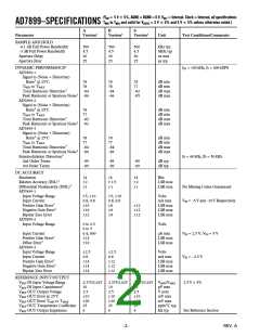
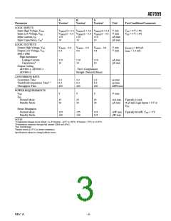
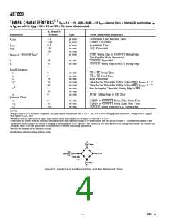
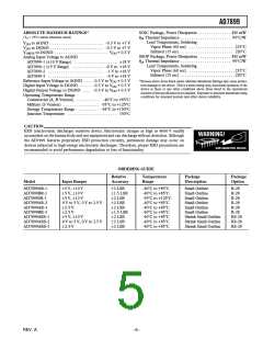
AD7899
PIN FUNCTION DESCRIPTIONS
Pin
No.
Mnemonic
Description
1
VREF
Reference Input/Output. This pin is provides access to the internal reference (2.5 V 20 mV) and
also allows the internal reference to be overdriven by an external reference source (2.5 V 5%).
A 0.1 µF decoupling capacitor should be connected between this pin and GND.
2, 6
3, 4
5
GND
Ground Pin. This pin should be connected to the system’s analog groundplane.
Analog Inputs. See Analog Input Section.
Positive Supply Voltage, 5.0 V 5%.
V
INB, VINA
VDD
7–13
14
DB13–DB7
OPGND
Data Bit 13 is the MSB, followed by Data Bit 12 to Data Bit 7. Three-state outputs.
Output Driver Ground. This is the ground pin of the output drivers for D13 to D0 and BUSY/EOC. It should
be connected to the system’s analog ground plane.
15
VDRIVE
This pin provides the positive supply voltage for the digital inputs and outputs. It is normally tied to VDD
but may also be powered by a 3 V 10% supply which allows the inputs and outputs to be interfaced
to 3 V processors and DSPs. VDRIVE should be decoupled with a 0.1 µF capacitor to GND.
16–22
DB6–DB0
Data Bit 6 to Data Bit 0. Three-state Outputs.
23
BUSY/EOC
BUSY/EOC Output. Digital output pin used to signify that a conversion is in progress or that a conversion
has finished. The function of the BUSY/EOC is determined by the state of CONVST at the end of con-
version. See the Timing and Control Section.
24
25
26
RD
Read Input. Active low logic input which is used in conjunction with CS low to enable the data outputs.
Chip Select Input. Active low logic input. The device is selected when this input is active.
Convert Start Input. Logic Input. A low to high transition on this input puts the track/hold into hold mode
and starts conversion.
CS
CONVST
27
CLKIN
Conversion Clock Input. CLKIN is an externally applied clock which allows the user to control the
conversion rate of the AD7899. If the CLKIN input is high on the rising edge of CONVST an externally
applied clock will be used as the conversion clock. If the CLKIN is low on the rising edge of CONVST
the internal laser-trimmed oscillator is used as the conversion clock. Each conversion needs sixteen clock
cycles in order for the conversion to be completed. The externally applied clock should have a duty cycle
no greater than 60/40. The CLKIN pin can be tied to GND if an external clock is not required.
28
STBY
Standby Mode Input. Logic input which is used to put the device into the power save or standby mode.
The STBY input is high for normal operation and low for standby operation.
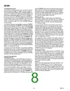
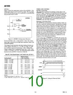
PIN CONFIGURATION
SOIC/SSOP
V
1
2
28
STBY
REF
27 CLKIN
26
GND
3
V
V
CONVST
INB
4
25
24
23
CS
INA
V
5
RD
DD
6
BUSY/EOC
GND
DB13
DB12
DB11
DB10
DB9
AD7899
TOP VIEW
(Not to Scale)
7
22 DB0
DB1
DB2
DB3
DB4
DB5
DB6
V
8
21
20
19
18
17
16
15
9
10
11
12
13
14
DB8
DB7
OPGND
DRIVE
–6–
REV. A

 ADI [ ADI ]