AD7899
t10
t9
CLKIN
t1
tACQ
tEOC
t8
CONVST
QUIET
TIME
t2
BUSY/EOC
tCONV
t5
RD
CS
t3
t4
THREE-STATE
THREE-STATE
t7
DATA
t6
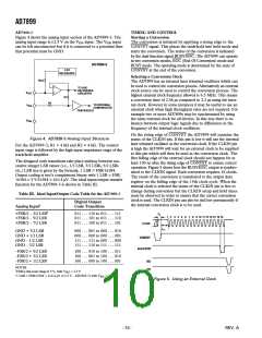
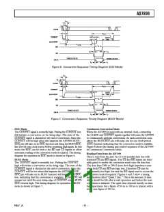
Figure 6. Conversion Sequence Timing Diagram (EOC Mode)
t10
t9
CLKIN
t1
tACQ
CONVST
t8
QUIET
TIME
BUSY/EOC
tCONV
t5
RD
CS
t3
t4
THREE-STATE
THREE-STATE
t7
DATA
t6
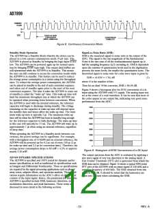
Figure 7. Conversion Sequence Timing Diagram (BUSY Mode)
EOC Mode
Continuous Conversion Mode
The CONVST signal is normally high. Pulsing the CONVST low
will initiate a conversion on its rising edge. The state of the
CONVST signal is checked at the end of conversion. Since the
CONVST will be high when this happens the AD7899 BUSY/
EOC pin will take on its EOC function and bring the BUSY/EOC
line low for one clock period before returning high again. In this
mode the EOC can be tied to the RD and CS signals to allow
automatic reading of the conversion result if required. The timing
diagram for operation in EOC mode is shown in Figure 6.
When the AD7899 is used with an external clock, connecting
the CLKIN and CONVST signals together will cause the AD7899
to continuously perform conversions. As each conversion com-
pletes the BUSY/EOC pin will pulse low for one clock period
(EOC function) indicating that the conversion result is available.
Figure 8 shows the timing and control sequence of the AD7899
in Continuous Conversion Mode.
Reading Data from the AD7899
Data is read from the part via a 14-bit parallel data bus with
standard CS and RD signals. The CS and RD inputs are inter-
nally gated to enable the conversion result onto the data bus.
The data lines DB0 to DB13 leave their high impedance state
when both CS and RD are logic low. Therefore CS may be
permanently tied logic low and the RD signal used to access the
conversion result if required. Figures 6 and 7 show a timing
specification called “Quiet Time.” This is the amount of time
which should be left after a read operation and before the next
conversion is initiated. The quiet time depends heavily on data
bus capacitance but a figure of 50 ns to 100 ns is typical, with a
worst case figure of 150 ns.
BUSY Mode
The CONVST signal is normally low. Pulsing the CONVST
high will initiate a conversion on its rising edge. The state of the
CONVST signal is checked at the end of conversion. Since the
CONVST will be low when this happens the AD7899 BUSY/
EOC pin will take on its BUSY function will bring BUSY/EOC
low, indicating that the conversion is complete. BUSY/EOC will
remain low until the next rising edge of CONVST where BUSY/
EOC returns high. The timing diagram for operation in BUSY
mode is shown in Figure 7.
–11–
REV. A

 ADI [ ADI ]