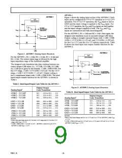
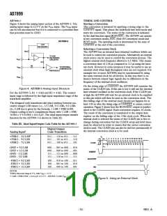
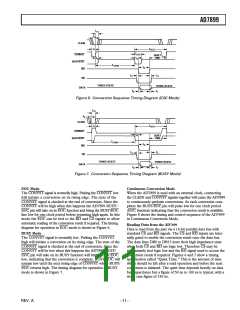
AD7899
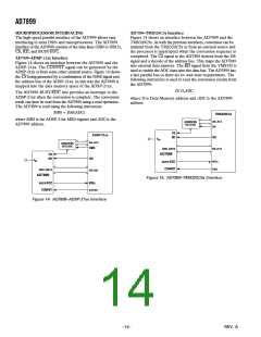
MICROPROCESSOR INTERFACING
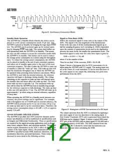
AD7899–TMS320C5x Interface
The high-speed parallel interface of the AD7899 allows easy
interfacing to most DSPs and microprocessors. The AD7899
interface of the AD7899 consists of the data lines (DB0 to DB13),
CS, RD, and BUSY/EOC.
Figure 15 shows an interface between the AD7899 and the
TMS320C5x. As with the previous interfaces, conversion can be
initiated from the TMS320C5x or from an external source and
the processor is interrupted when the conversion sequence is
completed. The CS signal to the AD7899 derived from the DS
signal and a decode of the address bus. This maps the AD7899
into external data memory. The RD signal from the TMS320 is
used to enable the ADC data onto the data bus. The AD7899 has
a fast parallel bus so there are no wait state requirements. The
following instruction is used to read the conversion results from
the AD7899:
AD7899–ADSP-21xx Interface
Figure 14 shows an interface between the AD7899 and the
ADSP-21xx. The CONVST signal can be generated by the
ADSP-21xx or from some other external source. Figure 14 shows
the CS being generated by a combination of the DMS signal and
the address bus of the ADSP-21xx. In this way the AD7899 is
mapped into the data memory space of the ADSP-21xx.
IN D,ADC
The AD7899 BUSY/EOC line provides an interrupt to the
ADSP-21xx when the conversion is complete. The conversion
result can then be read from the AD7899 using a read operation.
The AD7899 is read using the following instruction
where D is Data Memory address and ADC is the AD7899
address.
MR0 = DM(ADC)
TMS320C5x
where MR0 is the ADSP-21xx MR0 register and ADC is the
AD7899 address.
A0–A13
ADDRESS
DECODE
DS
CS
RD
ADSP-21xx
RD
V
IN
A0–A13
ADDRESS
DECODE
DMS
DB0–DB13
D0–D13
AD7899
BUSY/EOC
CONVST
CS
RD
RD
V
IN
INTn
PA0
DB0–DB13
D8–D21
AD7899
Figure 15. AD7899–TMS320C5x Interface
BUSY/EOC
IRQn
CONVST
DT1/F0
Figure 14. AD7899–ADSP-21xx Interface
–14–
REV. A

 ADI [ ADI ]