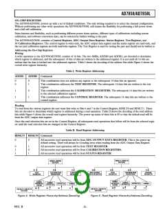
AD7858/AD7858L
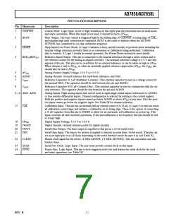
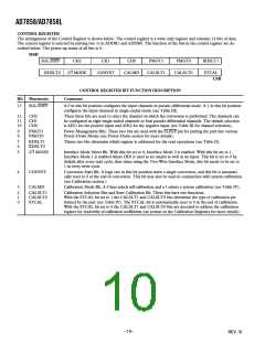
PIN FUNCTION DESCRIPTIONS
Pin Mnemonic
Description
Convert Start. Logic Input. A low to high transition on this input puts the track/hold into its hold mode
and starts conversion. When this input is not used, it should be tied to DVDD
1
CONVST
.
2
BUSY
Busy Output. The busy output is triggered high by the falling edge of CONVST or rising edge of CAL,
and remains high until conversion is completed. BUSY is also used to indicate when the AD7858/
AD7858L has completed its on-chip calibration sequence.
3
4
SLEEP
Sleep Input/Low-Power Mode. A Logic 0 initiates a sleep, and all circuitry is powered down including the
internal voltage reference provided there is no conversion or calibration being performed. Calibration
data is retained. A Logic 1 results in normal operation. See Power-Down section for more details.
Reference Input/Output. This pin is connected to the internal reference through a series resistor and is
the reference source for the analog-to-digital converter. The nominal reference voltage is 2.5 V and this
REFIN/REFOUT
appears at the pin. This pin can be overdriven by an external reference or can be taken as high as AVDD
When this pin is tied to AVDD, or when an externally applied reference approaches AVDD, the CREF1 pin
should also be tied to AVDD
.
.
5
6
7
AVDD
AGND
CREF1
Analog Positive Supply Voltage, +3.0 V to +5.5 V.
Analog Ground. Ground reference for track/hold, reference, and DAC.
Reference Capacitor (0.1 µF Multilayer Ceramic). This external capacitor is used as a charge source for
the internal DAC. The capacitor should be tied between the pin and AGND.
8
CREF2
Reference Capacitor (0.01 µF Ceramic Disc). This external capacitor is used in conjunction with the on-
chip reference. The capacitor should be tied between the pin and AGND.
9–16 AIN1–AIN8
Analog Inputs. Eight analog inputs that can be used as eight single-ended inputs (referenced to AGND)
or four pseudo-differential inputs. Channel configuration is selected by writing to the control register.
Both the positive and negative inputs cannot go below AGND or above AVDD at any time. Also the posi-
tive input cannot go below the negative input. See Table III for channel selection.
17
CAL
Calibration Input. This pin has an internal pull-up current source of 0.15 µA. A Logic 0 on this pin resets
all calibration control logic and initiates a calibration on its rising edge. There is the option of connecting
a 10 nF capacitor from this pin to DGND to allow for an automatic self-calibration on power-up. This
input overrides all other internal operations. If the autocalibration is not required, this pin should be tied
to a logic high.
18
19
20
21
DVDD
DGND
DOUT
DIN
Digital Supply Voltage, +3.0 V to +5.5 V.
Digital Ground. Ground reference point for digital circuitry.
Serial Data Output. The data output is supplied to this pin as a 16-bit serial word.
Serial Data Input. The data to be written is applied to this pin in serial form (16-bit word). This pin can
act as an input pin or as a I/O pin depending on the serial interface mode the part is in (see Table X).
22
CLKIN
Master clock signal for the device (4 MHz AD7858, 1.8 MHz AD7858L). Sets the conversion and cali-
bration times.
23
24
SCLK
SYNC
Serial Port Clock. Logic Input. The user must provide a serial clock on this input.
Frame Sync. Logic Input. This pin is level triggered active low and frames the serial clock for the read
and write operations (see Table IX).
REV. B
–7–

 ADI [ ADI ]