AD7858/AD7858L
TYPICAL TIMING DIAGRAMS
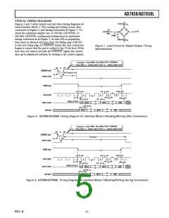
1.6mA
I
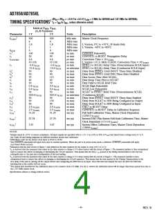
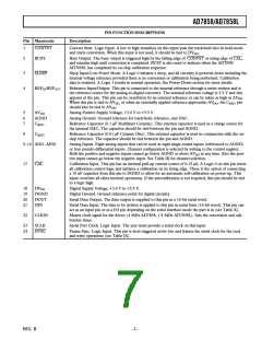
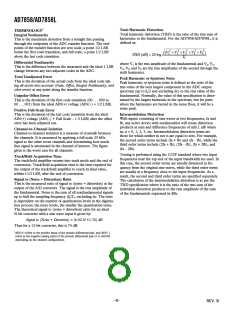
Figures 2 and 3 show typical read and write timing diagrams for
serial Interface Mode 2. The reading and writing occurs after
conversion in Figure 2, and during conversion in Figure 3. To
attain the maximum sample rate of 100 kHz (AD7858L) or
200 kHz (AD7858), reading and writing must be performed
during conversion as in Figure 3. At least 400 ns acquisition
time must be allowed (the time from the falling edge of BUSY
to the next rising edge of CONVST) before the next conversion
begins to ensure that the part is settled to the 12-bit level. If the
user does not want to provide the CONVST signal, the conver-
sion can be initiated in software by writing to the control register.
OL
TO
OUTPUT
PIN
+2.1V
C
L
100pF
200A
I
OH
Figure 1. Load Circuit for Digital Output Timing
Specifications
tCONVERT = 4.6s MAX, 10s MAX FOR L VERSION
t1 = 100ns MIN, t4 = 50/90ns MAX 5V/3V, t7 = 40/60ns MIN 5V/3V
t1
CONVST (I/P)
tCONVERT
t2
BUSY (O/P)
SYNC (I/P)
t3
t11
t9
1
5
6
16
SCLK (I/P)
DOUT (O/P)
DIN (I/P)
t4
t10
t12
t6
t6
DB11
THREE-STATE
THREE-
STATE
DB15
DB0
t8
t7
DB15
DB11
DB0
Figure 2. AD7858/AD7858L Timing Diagram for Interface Mode 2 (Reading/Writing After Conversion)
tCONVERT = 4.6s MAX, 10s MAX FOR L VERSION
t1 = 100ns MIN, t4 = 50/90ns MAX 5V/3V, t7 = 40/60ns MIN 5V/3V
t1
CONVST (I/P)
tCONVERT
t2
BUSY (O/P)
SYNC (I/P)
t3
t11
t9
1
5
6
16
SCLK (I/P)
DOUT (O/P)
DIN (I/P)
t4
t10
t12
t6
t6
THREE-STATE
THREE-
STATE
DB15
DB11
DB0
t8
t7
DB15
DB11
DB0
Figure 3. AD7858/AD7858L Timing Diagram for Interface Mode 2 (Reading/Writing During Conversion)
REV. B
–5–

 ADI [ ADI ]