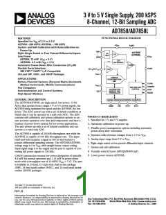
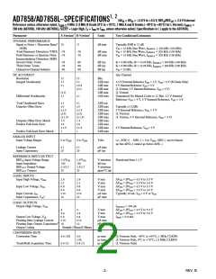
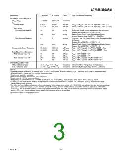
AD7858/AD7858L
(AVDD = DVDD = +3.0 V to +5.5 V; fCLKIN = 4 MHz for AD7858 and 1.8/1 MHz for AD7858L;
TA = TMIN to TMAX , unless otherwise noted)
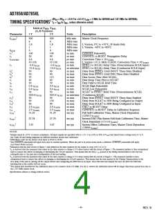
TIMING SPECIFICATIONS1
Limit at TMIN, TMAX
(A, B Versions)
3 V
Parameter
5 V
Units
Description
2
fCLKIN
500
4
1.8
1
4
100
50
4.6
10 (18)
–0.4 tSCLK
ϯ0.4 tSCLK
50
500
4
1.8
1
4
100
90
4.6
10 (18)
–0.4 tSCLK
ϯ0.4 tSCLK
90
90
115
60
30
0.4 tSCLK
0.4 tSCLK
50
50/0.4 tSCLK
50
130
90
kHz min
MHz max
MHz max
MHz max
MHz max
ns min
Master Clock Frequency
L Version, 0°C to +70°C, B Grade Only
L Version, –40°C to +85°C
fSC3 LK
t1
CONVST Pulsewidth
CONVST↓ to BUSY↑ Propagation Delay
Conversion Time = 18 tCLKIN
L Version 1.8 (1) MHz CLKIN. Conversion Time = 18 tCLKIN
SYNC↓ to SCLK↓ Setup Time (Noncontinuous SCLK Input)
t2
ns max
tCONVERT
µs max
µs max
t3
ns min
ns min/max SYNC↓ to SCLK↓ Setup Time (Continuous SCLK Input)
4
t44
ns max
ns max
ns max
ns min
ns min
ns min
ns min
ns min
Delay from SYNC↓ Until DOUT Three-State Disabled
Delay from SYNC↓ Until DIN Three-State Disabled
Data Access Time After SCLK↓
Data Setup Time Prior to SCLK↑
Data Valid to SCLK Hold Time
SCLK High Pulsewidth
SCLK Low Pulsewidth
SCLK↑ to SYNC↑ Hold Time (Noncontinuous SCLK)
t54
50
75
40
20
t6
t7
t8
t9
t10
0.4 tSCLK
0.4 tSCLK
30
30/0.4 tSCLK
50
90
50
2.5 tCLKIN
2.5 tCLKIN
31.25
t11
ns min/max (Continuous SCLK)
5
t12
ns max
ns max
ns max
ns max
ns max
ms typ
Delay from SYNC↑ Until DOUT Three-State Enabled
t13
t14
Delay from SCLK↑ to DIN Being Configured as Output
Delay from SCLK↑ to DIN Being Configured as Input
CAL↑ to BUSY↑ Delay
6
t15
2.5 tCLKIN
2.5 tCLKIN
31.25
t16
tCAL
CONVST↓ to BUSY↑ Delay in Calibration Sequence
Full Self-Calibration Time, Master Clock Dependent
7
(125013 tCLKIN
Internal DAC Plus System Full-Scale Calibration Time, Master
Clock Dependent (111114 tCLKIN
System Offset Calibration Time, Master Clock Dependent
(13899 tCLKIN
)
7
tCAL1
27.78
3.47
27.78
3.47
ms typ
ms typ
)
7
tCAL2
)
NOTES
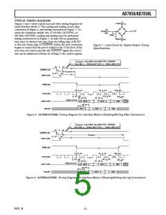
1Sample tested at +25°C to ensure compliance. All input signals are specified with tr = tf = 5 ns (10% to 90% of VDD) and timed from a voltage level of 1.6 V.
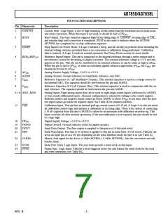
See Table XI and timing diagrams for different interface modes and Calibration.
2Mark/Space ratio for the master clock input is 40/60 to 60/40.
3The CONVST pulsewidth will apply here only for normal operation. When the part is in power-down mode, a different CONVST pulsewidth will apply
(see Power-Down section).
4Measured with the load circuit of Figure 1 and defined as the time required for the output to cross 0.8 V or 2.4 V.
5t12 is derived form the measured time taken by the data outputs to change 0.5 V when loaded with the circuit of Figure 1. The measured number is then extrapolated
back to remove the effects of charging or discharging the 100 pF capacitor. This means that the time, t12, quoted in the timing characteristics is the true bus
relinquish time of the part and is independent of the bus loading.
6t14 is derived form the measured time taken by the data outputs to change 0.5 V when loaded with the circuit of Figure 1. The measured number is then
extrapolated back to remove the effects of charging or discharging the 100 pF capacitor. This means that the time quoted in the Timing Characteristics is the
true delay of the part in turning off the output drivers and configuring the DIN line as an input. Once this time has elapsed the user can drive the DIN line
knowing that a bus conflict will not occur.
7The typical time specified for the calibration times is for a master clock of 4 MHz. For the L version the calibration times will be longer than those quoted here due to
the 1.8/1 MHz master clock.
Specifications subject to change without notice.
–4–
REV. B

 ADI [ ADI ]