AD7858/AD7858L
ABSOLUTE MAXIMUM RATINGS1
SOIC, SSOP Package, Power Dissipation . . . . . . . . . . 450 mW
(TA = +25°C unless otherwise noted)
θ
JA Thermal Impedance . . . 75°C/W (SOIC) 115°C/W (SSOP)
θ
JC Thermal Impedance . . . . 25°C/W (SOIC) 35°C/W (SSOP)
AVDD to AGND . . . . . . . . . . . . . . . . . . . . . . . –0.3 V to +7 V
DVDD to DGND . . . . . . . . . . . . . . . . . . . . . . . –0.3 V to +7 V
AVDD to DVDD . . . . . . . . . . . . . . . . . . . . . . . –0.3 V to +0.3 V
Analog Input Voltage to AGND . . . . –0.3 V to AVDD + 0.3 V
Digital Input Voltage to DGND . . . . –0.3 V to DVDD + 0.3 V
Digital Output Voltage to DGND . . . –0.3 V to DVDD + 0.3 V
REFIN/REFOUT to AGND . . . . . . . . . –0.3 V to AVDD + 0.3 V
Lead Temperature, Soldering
Vapor Phase (60 sec) . . . . . . . . . . . . . . . . . . . . . . +215°C
Infrared (15 sec) . . . . . . . . . . . . . . . . . . . . . . . . . . +220°C
NOTES
1Stresses above those listed under Absolute Maximum Ratings may cause perma-
nent damage to the device. This is a stress rating only; functional operation of the
device at these or any other conditions above those listed in the operational
sections of this specification is not implied. Exposure to absolute maximum rating
conditions for extended periods may affect device reliability.
Input Current to Any Pin Except Supplies2 . . . . . . .
Operating Temperature Range
Commercial (A, B Versions) . . . . . . . . . . . –40°C to +85°C
Storage Temperature Range . . . . . . . . . . . –65°C to +150°C
Junction Temperature . . . . . . . . . . . . . . . . . . . . . . . . . +150°C
Plastic DIP Package, Power Dissipation . . . . . . . . . . 450 mW
10 mA
2Transient currents of up to 100 mA will not cause SCR latch-up.
θ
JA Thermal Impedance . . . . . . . . . . . . . . . . . . . . . 105°C/W
θ
JC Thermal Impedance . . . . . . . . . . . . . . . . . . . . 34.7°C/W
Lead Temperature, (Soldering, 10 sec) . . . . . . . . . . +260°C
CAUTION
ESD (electrostatic discharge) sensitive device. Electrostatic charges as high as 4000 V readily
accumulate on the human body and test equipment and can discharge without detection. Although
the AD7858/AD7858L features proprietary ESD protection circuitry, permanent damage may
occur on devices subjected to high-energy electrostatic discharges. Therefore, proper ESD precautions
are recommended to avoid performance degradation or loss of functionality.
WARNING!
ESD SENSITIVE DEVICE
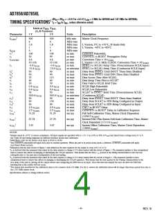
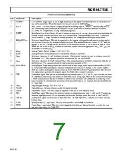
PIN CONFIGURATIONS
DIP, SOIC, AND SSOP
ORDERING GUIDE
Linearity Power
Error
Dissipation Package
(mW)
Model
(LSB)1
Options2
1
24
CONVST
BUSY
SYNC
2
3
23
22
SCLK
AD7858AN
1
1/2
1
1
1
1/2
1
1
1
20
20
6.85
6.85
20
N-24
N-24
N-24
N-24
R-24
R-24
R-24
R-24
RS-24
SLEEP
CLKIN
AD7858BN
REF /REF
IN
4
5
21 DIN
AD7858LAN3
AD7858LBN3
AD7858AR
OUT
AD7858/
AD7858L
AV
20 DOUT
DD
AGND
6
19
18
DGND
TOP VIEW
(Not to Scale)
C
7
DV
DD
REF1
AD7858BR
20
C
8
17 CAL
AD7858LAR3
AD7858LBR3
AD7858LARS3
EVAL-AD7858CB4
EVAL-CONTROL BOARD5
6.85
6.85
6.85
REF2
AIN1
AIN8
16
9
10
11
AIN2
AIN3
AIN7
AIN6
15
14
13
AIN4 12
AIN5
NOTES
1Linearity error here refers to integral linearity error.
2N = Plastic DIP; R = SOIC; RS = SSOP.
3L signifies the low-power version.
4This can be used as a stand-alone evaluation board or in conjunction with the EVAL-
CONTROL BOARD for evaluation/demonstration purposes.
5This board is a complete unit allowing a PC to control and communicate with all
Analog Devices evaluation boards ending in the CB designators.
–6–
REV. B

 ADI [ ADI ]