AD7858/AD7858L
ON-CHIP REGISTERS
The AD7858/AD7858L powers up with a set of default conditions. The only writing required is to select the channel configuration.
Without performing any other write operations the AD7858/AD7858L still retains the flexibility for performing a full power-down
and a full self-calibration.
Extra features and flexibility, such as performing different power-down options, different types of calibrations including system
calibration, and software conversion start, can be selected by further writing to the part.
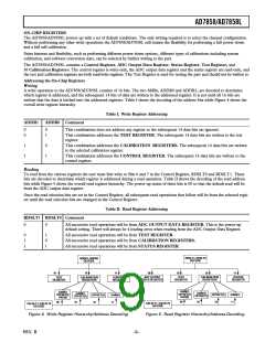
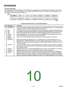
The AD7858/AD7858L contains a Control Register, ADC Output Data Register, Status Register, Test Register, and
10 Calibration Registers. The control register is write-only, the ADC output data register and the status register are read-only, and
the test and calibration registers are both read/write registers. The Test Register is used for testing the part and should not be written to.
Addressing the On-Chip Registers
Writing
A write operation to the AD7858/AD7858L consists of 16 bits. The two MSBs, ADDR0 and ADDR1, are decoded to determine
which register is addressed, and the subsequent 14 bits of data are written to the addressed register. It is not until all 16 bits are
written that the data is latched into the addressed registers. Table I shows the decoding of the address bits while Figure 4 shows the
overall write register hierarchy.
Table I. Write Register Addressing
ADDR1
ADDR0 Comment
0
0
0
1
This combination does not address any register so the subsequent 14 data bits are ignored.
This combination addresses the TEST REGISTER. The subsequent 14 data bits are written to the test
register.
1
1
0
1
This combination addresses the CALIBRATION REGISTERS. The subsequent 14 data bits are written
to the selected calibration register.
This combination addresses the CONTROL REGISTER. The subsequent 14 data bits are written to the
control register.
Reading
To read from the various registers the user must first write to Bits 6 and 7 in the Control Register, RDSLT0 and RDSLT1. These
bits are decoded to determine which register is addressed during a read operation. Table II shows the decoding of the read address
bits while Figure 5 shows the overall read register hierarchy. The power-up status of these bits is 00 so that the default read will be
from the ADC output data register.
Once the read selection bits are set in the Control Register, all subsequent read operations that follow will be from the selected regis-
ter until the read selection bits are changed in the Control Register.
Table II. Read Register Addressing
RDSLT1 RDSLT0 Comment
0
0
All successive read operations will be from ADC OUTPUT DATA REGISTER. This is the power-up
default setting. There will always be 4 leading zeros when reading from the ADC Output Data Register.
0
1
1
1
0
1
All successive read operations will be from TEST REGISTER.
All successive read operations will be from CALIBRATION REGISTERS.
All successive read operations will be from STATUS REGISTER.
RDSLT1, RDSLT0
DECODE
ADDR1, ADDR0
DECODE
00
01
10
11
01
10
11
ADC OUTPUT
DATA REGISTER
TEST
REGISTER
CALIBRATION
REGISTERS
STATUS
REGISTER
TEST
REGISTER
CALIBRATION
REGISTERS
CONTROL
REGISTER
GAIN(1)
OFFSET(1)
DAC(8)
GAIN(1)
OFFSET(1)
DAC(8)
GAIN(1)
GAIN(1)
OFFSET(1)
10
GAIN(1)
11
OFFSET(1)
10
GAIN(1)
11
OFFSET(1)
OFFSET(1)
00
01
00
01
CALSLT1, CALSLT0
DECODE
CALSLT1, CALSLT0
DECODE
Figure 4. Write Register Hierarchy/Address Decoding
Figure 5. Read Register Hierarchy/Address Decoding
REV. B
–9–

 ADI [ ADI ]