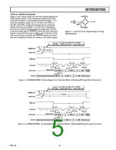
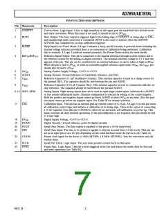
AD7858/AD7858L
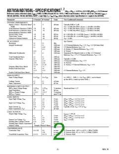
Parameter
A Version1
B Version1
Units
Test Conditions/Comments
DYNAMIC PERFORMANCE
AVDD, DVDD
+3.0/+5.5
+3.0/+5.5
V min/max
IDD
Normal Mode5
6 (1.9)
5.5 (1.9)
6 (1.9)
5.5 (1.9)
mA max
mA max
AVDD = DVDD = 4.5 V to 5.5 V. Typically 4.5 mA (1.5)
AVDD = DVDD = 3.0 V to 3.6 V. Typically 4.0 mA (1.5 mA)
Sleep Mode6
With External Clock On
10
400
5
10
400
5
µA typ
µA typ
µA max
Full Power-Down. Power Management Bits in Control
Register Set as PMGT1 = 1, PMGT0 = 0
Partial Power-Down. Power Management Bits in
Control Register Set as PMGT1 = 1, PMGT0 = 1
Typically 1 µA. Full Power-Down. Power Management Bits
in Control
With External Clock Off
Register Set as PMGT1 = 1, PMGT0 = 0
Partial Power-Down. Power Management Bits in Control
Register Set as PMGT1 = 1, PMGT0 = 1
200
200
µA typ
Normal-Mode Power Dissipation
33 (10.5)
20 (6.85)
33 (10.5)
20 (6.85)
mW max
mW max
V
DD = 5.5 V. Typically 25 mW (8); SLEEP = VDD
VDD = 3.6 V. Typically 15 mW (5.4); SLEEP = VDD
Sleep Mode Power Dissipation
With External Clock On
55
36
27.5
18
55
36
27.5
18
µW typ
µW typ
µW max
µW max
V
V
V
DD = 5.5 V. SLEEP = 0 V
DD = 3.6 V. SLEEP = 0 V
DD = 5.5 V. Typically 5.5 µW; SLEEP = 0 V
With External Clock Off
VDD = 3.6 V. Typically 3.6 µW; SLEEP = 0 V
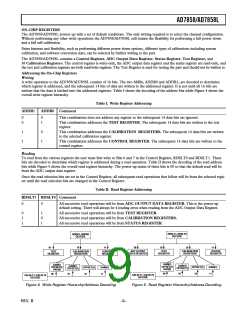
SYSTEM CALIBRATION
Offset Calibration Span7
Gain Calibration Span7
+0.05 × VREF/–0.05 × VREF
+1.025 × VREF/–0.975 × VREF
V max/min Allowable Offset Voltage Span for Calibration
V max/min Allowable Full-Scale Voltage Span for Calibration
NOTES
1Temperature ranges as follows: A, B Versions: –40°C to +85°C. For L Versions, A and B Versions fCLKIN = 1 MHz over –40°C to +85°C temperature range,
B Version fCLKIN = 1.8 MHz over 0°C to +70°C temperature range.
2Specifications apply after calibration.
3SNR calculation includes distortion and noise components.
4Sample tested @ +25°C to ensure compliance.
5All digital inputs @ DGND except for CONVST, SLEEP, CAL, and SYNC @ DVDD. No load on the digital outputs. Analog inputs @ AGND.
6CLKIN @ DGND when external clock off. All digital inputs @ DGND except for CONVST, SLEEP, CAL, and SYNC @ DVDD. No load on the digital
outputs. Analog inputs @ AGND.
7The Offset and Gain Calibration Spans are defined as the range of offset and gain errors that the AD7858/AD7858L can calibrate. Note also that these are voltage
spans and are not absolute voltages ( i.e., the allowable system offset voltage presented at AIN(+) for the system offset error to be adjusted out will be AIN(–)
0.05 × VREF, and the allowable system full-scale voltage applied between AIN(+) and AIN(–) for the system full-scale voltage error to be adjusted out will be
VREF 0.025 × VREF). This is explained in more detail in the Calibration section of the data sheet.
Specifications subject to change without notice.
REV. B
–3–

 ADI [ ADI ]