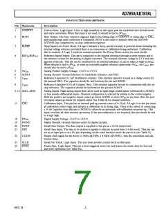
AD7858/AD7858L
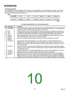
CONTROL REGISTER
The arrangement of the Control Register is shown below. The control register is a write only register and contains 14 bits of data.
The control register is selected by putting two 1s in ADDR1 and ADDR0. The function of the bits in the control register are de-
scribed below. The power-up status of all bits is 0.
MSB
SGL/DIFF
CH2
CH1
CH0
PMGT1
PMGT0
RDSLT1
STCAL
RDSLT0
2/3 MODE
CONVST
CALMD
CALSLT1
CALSLT0
LSB
CONTROL REGISTER BIT FUNCTION DESCRIPTION
Comment
Bit
Mnemonic
13
SGL/DIFF
A 0 in this bit position configures the input channels in pseudo-differential mode. A 1 in this bit position
configures the input channels in single-ended mode (see Table III).
12
11
10
CH2
CH1
CH0
These three bits are used to select the channel on which the conversion is performed. The channels can
be configured as eight single-ended channels or four pseudo-differential channels. The default selection
is AIN1 for the positive input and AIN2 for the negative input (see Table III for channel selection).
9
8
PMGT1
PMGT0
Power Management Bits. These two bits are used with the SLEEP pin for putting the part into various
Power-Down Modes (see Power-Down section for more details).
7
6
RDSLT1
RDSLT0
Theses two bits determine which register is addressed for the read operations (see Table II).
5
2/3 MODE
Interface Mode Select Bit. With this bit set to 0, Interface Mode 2 is enabled. With this bit set to 1,
Interface Mode 1 is enabled where DIN is used as an output as well as an input. This bit is set to 0 by
default after every read cycle; thus when using the Two-Wire Interface Mode, this bit needs to be set to
1 in every write cycle.
4
3
CONVST
CALMD
Conversion Start Bit. A logic one in this bit position starts a single conversion, and this bit is automati-
cally reset to 0 at the end of conversion. This bit may also be used in conjunction with system calibration
(see Calibration section.)
Calibration Mode Bit. A 0 here selects self-calibration, and a 1 selects a system calibration (see Table IV).
2
1
0
CALSLT1
CALSLT0
STCAL
Calibration Selection Bits and Start Calibration Bit. These bits have two functions.
With the STCAL bit set to 1 the CALSLT1 and CALSLT0 bits determine the type of calibration per
formed by the part (see Table IV). The STCAL bit is automatically reset to 0 at the end of calibration.
With the STCAL bit set to 0 the CALSLT1 and CALSLT0 bits are decoded to address the calibration
register for read/write of calibration coefficients (see section on the Calibration Registers for more details).
–10–
REV. B

 ADI [ ADI ]