AD7858/AD7858L
Table VI. Power Management Options
PMGT1 PMGT0 SLEEP
a logic high. If the autocalibration is disabled, then the user must
take into account the time required by the AD7858 to power-up
before a self-calibration is carried out. This power-up time is the
time taken for the AD7858 to power up when power is first
applied (300 µs) typ) or the time it takes the external reference
to settle to the 12-bit level–whichever is the longer.
Bit
Bit
Pin
Comment
0
0
0
Full Power-Down if Not
Calibrating or Converting
(Default Condition
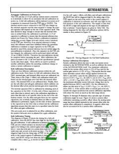
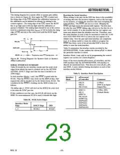
The AD7858 powers up from a full hardware or software
power-down in 5 µs typ. This limits the throughput which the
part is capable of to 104 kSPS for the AD7858 operating with a
4 MHz CLK and 66 kSPS for the AD7858L with a 1.8 MHz
CLK when powering down between conversions. Figure 22
shows how power-down between conversions is implemented
using the CONVST pin. The user first selects the power-down
between conversions option by using the SLEEP pin and the
power management bits, PMGT1 and PMGT0, in the control
register, (see last section). In this mode the AD7858 automati-
cally enters a full power-down at the end of a conversion, i.e.,
when BUSY goes low. The falling edge of the next CONVST
pulse causes the part to power up. Assuming the external refer-
ence is left powered up, the AD7858 should be ready for normal
operation 5 µs after this falling edge. The rising edge of CONVST
initiates a conversion so the CONVST pulse should be at least
5 µs wide. The part automatically powers down on completion
of the conversion.
After Power-On)
0
0
0
1
1
X
Normal Operation
Normal Operation
(Independent of the SLEEP Pin)
Full Power-Down
Partial Power-Down if Not
Converting
1
1
0
1
X
X
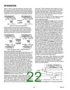
A typical connection diagram for a low power application is
shown in Figure 21 (AD7858L is the low power version of the
AD7858).
CURRENT,
I = 1.5mA
TYP
1.8MHz
OSCILLATOR
0.1F
ANALOG
SUPPLY
+3V
10F 0.1F
MASTER
AV
DV
100kHz
PULSE
GENERATOR
CLOCK
INPUT
DD
DD
START CONVERSION ON RISING EDGE
POWER-UP ON FALLING EDGE
0V TO 2.5V
INPUT
AIN(+)
CLKIN
AIN(–)
AD7858/
AD7858L
5s
C
REF1
CONVERSION
START INPUT
0.1F
CONVST
CONVST
t
CONVERT
C
REF2
SERIAL CLOCK
INPUT
0.01F
BUSY
SCLK
AUTO POWER
DOWN AFTER
CONVERSION
SLEEP
CAL
POWER-UP
TIME
NORMAL
FULL
POWER-UP
TIME
SYNC
OPERATION POWER-DOWN
LOW
POWER
C/P
SERIAL DATA
OUTPUT
0.01F
Figure 22. Power-Up Timing When Using CONVST Pin
DOUT
DIN
AUTO CAL
ON
POWER-UP
NOTE: Where the software CONVST is used or automatic full
power-down, the part must be powered up in software with an
extra write setting PMGT1 = 0 and PMGT0 = 1 before a con-
version is initiated in the next write. Automatic partial power-
down after a calibration is not possible; the part must be
powered down manually. If software calibrations are to be used
when operating in the partial power-down mode, then three
separate writes are required. The first initiates the type of cali-
bration required, the second write powers the part down into
partial power-down mode, while the third write powers the part
up again before the next calibration command is issued.
AGND
DGND
SERIAL DATA
INPUT
REF /REF
IN
OUT
INTERNAL
REFERENCE
0.1F
OPTIONAL
EXTERNAL
REFERENCE
REF192
Figure 21. Typical Low Power Circuit
Using the Internal (On-Chip) Reference
POWER-UP TIMES
As in the case of an external reference, the AD7858 can power-
up from one of two conditions, power-up after the supplies are
connected or power-up from hardware/software power-down.
When using the on-chip reference and powering up when AVDD
and DVDD are first connected, it is recommended that the power-
up calibration mode be disabled as explained above. When using
the on-chip reference, the power-up time is effectively the time
it takes to charge up the external capacitor on the REFIN/REFOUT
pin. This time is given by the equation:
Using an External Reference
When the AD7858 is powered up, the part is powered up from
one of two conditions. First, when the power supplies are ini-
tially powered up and, secondly, when the part is powered up
from either a hardware or software power-down (see last section).
When AVDD and DVDD are powered up, the AD7858 should be
left idle for approximately 32 ms (4 MHz CLK) to allow for the
autocalibration if a 10 nF cap is placed on the CAL pin, (see
Calibration section). During power-up the functionality of the
SLEEP pin is disabled, i.e., the part will not power down until
the end of the calibration if SLEEP is tied logic low. The auto-
calibration on power-up can be disabled if the CAL pin is tied to
t
UP = 9 × R × C
where R ≅ 150 kΩ and C = external capacitor.
REV. B
–19–

 ADI [ ADI ]