AD7858/AD7858L
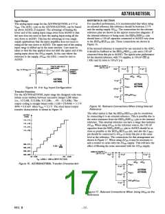
REFERENCE SECTION
Input Range
For specified performance, it is recommended that when using
an external reference this reference should be between 2.3 V
and the analog supply AVDD. The connections for the relevant
reference pins are shown in the typical connection diagrams. If
the internal reference is being used, the REFIN/REFOUT pin
should have a 100 nF capacitor connected to AGND very close
to the REFIN/REFOUT pin. These connections are shown in
Figure 16.
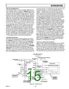
The analog input range for the AD7858/AD7858L is 0 V to
V
REF. The AIN(–) pin on the AD7858/AD7858L can be biased
up above AGND, if required. The advantage of biasing the
lower end of the analog input range away from AGND is that
the user does not need to have the analog input swing all the
way down to AGND. This has the advantage in true single-
supply applications that the input amplifier does not need to
swing all the way down to AGND. The upper end of the analog
input range is shifted up by the same amount. Care must be
taken so that the bias applied does not shift the upper end of the
analog input above the AVDD supply. In the case where the
reference is the supply, AVDD, the AIN(–) must be tied to
AGND.
If the internal reference is required for use external to the ADC,
it should be buffered at the REFIN/REFOUT pin and a 100 nF
connected from this pin to AGND. The typical noise performance
for the internal reference, with 5 V supplies, is 150 nV/√Hz @
1 kHz and dc noise is 100 µV p-p.
ANALOG SUPPLY
+3V TO +5V
TRACK AND HOLD
AIN(+)
AMPLIFIER
10F
0.1F
0.1F
V
= 0 TO V
REF
STRAIGHT
BINARY
FORMAT
IN
DOUT
AIN(–)
AV
DD
DV
DD
C
C
REF1
AD7858/
AD7858L
0.1F
AD7858/
AD7858L
REF2
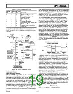
Figure 14. 0 to VREF Input Configuration
0.01F
0.1F
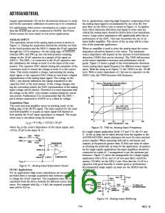
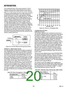
Transfer Function
For the AD7858/AD7858L input range the designed code tran-
sitions occur midway between successive integer LSB values
(i.e., 1/2 LSB, 3/2 LSBs, 5/2 LSBs . . . FS – 3/2 LSBs). The
output coding is straight binary with 1 LSB = FS/4096 = 3.3 V/
4096 = 0.8 mV when VREF = 3.3 V. The ideal input/output
transfer characteristic is shown in Figure 15.
REF /REF
IN
OUT
Figure 16. Relevant Connections When Using Internal
Reference
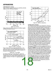
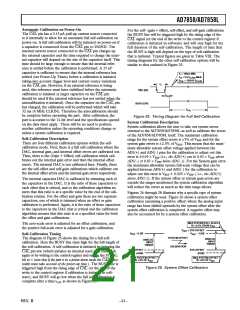
The other option is that the REFIN/REFOUT pin be overdriven
by connecting it to an external reference. This is possible due to
the series resistance from the REFIN/REFOUT pin to the internal
reference. This external reference can have a range that includes
AVDD. When using AVDD as the reference source, the 100 nF
capacitor from the REFIN/REFOUT pin to AGND should be as
close as possible to the REFIN/REFOUT pin, and also the CREF1
pin should be connected to AVDD to keep this pin at the same
level as the reference. The connections for this arrangement are
shown in Figure 17. When using AVDD it may be necessary to
add a resistor in series with the AVDD supply. This will have the
effect of filtering the noise associated with the AVDD supply.
OUTPUT
CODE
111...111
111...110
111...101
111...100
000...011
FS
4096
1LSB =
000...010
000...001
000...000
ANALOG SUPPLY
+3V TO +5V
10F
0.1F
0.1F
0V 1LSB
+FS –1LSB
= (AIN(+) – AIN(–)), INPUT VOLTAGE
V
IN
AV
DV
DD
DD
Figure 15. AD7858/AD7858L Transfer Characteristic
C
C
REF1
0.1F
AD7858/
AD7858L
REF2
0.01F
0.1F
REF /REF
IN
OUT
Figure 17. Relevant Connections When Using AVDD as the
Reference
REV. B
–17–

 ADI [ ADI ]