AD7858/AD7858L
CIRCUIT INFORMATION
conversion will take 17.5 CLKIN periods. The maximum speci-
The AD7858/AD7858L is a fast, 12-bit single supply A/D con-
verter. The part requires an external 4 MHz/1.8 MHz master
clock (CLKIN), two CREF capacitors, a CONVST signal to start
conversion, and power supply decoupling capacitors. The part
provides the user with track/hold, on-chip reference, calibration
features, A/D converter, and serial interface logic functions on a
single chip. The A/D converter section of the AD7858/AD7858L
consists of a conventional successive-approximation converter
based around a capacitor DAC. The AD7858/AD7858L accepts
an analog input range of 0 to +VDD where the reference can be
tied to VDD. The reference input to the part is buffered on-chip.
fied conversion time is 4.6 µs for the AD7858 (18tCLKIN
,
CLKIN = 4 MHz) and 10 µs for the AD7858L (18tCLKIN
,
CLKIN = 1.8 MHz). When a conversion is completed, the
BUSY output goes low, and then the result of the conversion
can be read by accessing the data through the serial interface.
To obtain optimum performance from the part, the read opera-
tion should not occur during the conversion or 400 ns prior to
the next CONVST rising edge. However, the maximum
throughput rates are achieved by reading/writing during conver-
sion, and reading/writing during conversion is likely to degrade
the Signal to (Noise + Distortion) by only 0.5 dBs. The AD7858
can operate at throughput rates up to 200 kHz, 100 kHz for the
AD7858L. For the AD7858 a conversion takes 18 CLKIN
periods; 2 CLKIN periods are needed for the acquisition time
giving a full cycle time of 5 µs (= 200 kHz, CLKIN = 4 MHz).
For the AD7858L 100 kHz throughput can be obtained as
follows: the CLKIN and CONVST signals are arranged to give
a conversion time of 16.5 CLKIN periods as described above,
1.5 CLKIN periods are allowed for the acquisition time. This
gives a full cycle time of 10 µs (=100 kHz, CLKIN = 1.8 MHz).
When using the software conversion start for maximum through-
put the user must ensure the control register write operation
extends beyond the falling edge of BUSY. The falling edge of
BUSY resets the CONVST bit to 0 and allows it to be repro-
grammed to 1 to start the next conversion.
A major advantage of the AD7858/AD7858L is that a conversion
can be initiated in software as well as applying a signal to the
CONVST pin. Another innovative feature of the AD7858/
AD7858L is self-calibration on power-up, which is initiated
having a capacitor from the CAL pin to AGND, to give superior
dc accuracy. See Automatic Calibration on Power-Up section.
The part is available in a 24-pin SSOP package and this offers
the user considerable space-saving advantages over alternative
solutions. The AD7858L version typically consumes only
5.5 mW making it ideal for battery-powered applications.
CONVERTER DETAILS
The master clock for the part must be applied to the CLKIN
pin. Conversion is initiated on the AD7858/AD7858L by pulsing
the CONVST input or by writing to the control register and
setting the CONVST bit to 1. On the rising edge of CONVST
(or at the end of the control register write operation), the on-
chip track/hold goes from track to hold mode. The falling edge
of the CLKIN signal that follows the rising edge of the CONVST
signal initiates the conversion, provided the rising edge of
CONVST occurs at least 10 ns typically before this CLKIN
edge. The conversion cycle will take 16.5 CLKIN periods from
this CLKIN falling edge. If the 10 ns setup time is not met, the
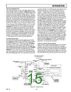
TYPICAL CONNECTION DIAGRAM
Figure 10 shows a typical connection diagram for the AD7858/
AD7858L. The AGND and the DGND pins are connected
together at the device for good noise suppression. The CAL pin
has a 0.01 µF capacitor to enable an automatic self-calibration
on power-up. The conversion result is output in a 16-bit word
with four leading zeros followed by the MSB of the 12-bit result.
Note that after the AVDD and DVDD power-up the part will
4MHz/1.8MHz OSCILLATOR
200kHz/100kHz PULSE GENERATOR
MASTER CLOCK
INPUT
0.1F
ANALOG SUPPLY
+3V TO +5V
10F
0.1F
CONVERSION
START INPUT
AV
DD
DV
DD
OSCILLOSCOPE
CLKIN
SCLK
AIN(+)
AIN(–)
0V TO 2.5V
INPUT
CH1
CH2
SERIAL CLOCK
INPUT
C
REF1
REF2
CONVST
SYNC
DIN
0.1F
0.01F
AD7858/
AD7858L
C
CH3
CH4
CH5
FRAME SYNC INPUT
SERIAL DATA INPUT
DV
DD
SLEEP
CAL
0.01F
DOUT
AGND
DGND
SERIAL DATA
OUTPUT
AUTO CAL ON
POWER-UP
4 LEADING
ZEROS FOR
ADC DATA
INTERNAL/
EXTERNAL
REFERENCE
DATA GENERATOR
0.1F
OPTIONAL
AD780/
REF-192
EXTERNAL
PULSE GENERATOR
REFERENCE
Figure 10. Typical Circuit
–15–
REV. B

 ADI [ ADI ]