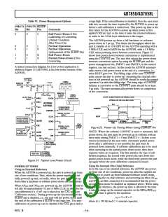
AD7858/AD7858L
require approximately 150 ms for the internal reference to settle
and for the automatic calibration on power-up to be completed.
For ac applications, removing high frequency components from
the analog input signal is recommended by use of an RC low-
pass filter on the AIN(+) pin as shown in Figure 13. In applica-
tions where harmonic distortion and signal to noise ratio are
critical the analog input should be driven from a low impedance
source. Large source impedances will significantly affect the ac
performance of the ADC. This may necessitate the use of an
input buffer amplifier. The choice of the op amp will be a func-
tion of the particular application.
For applications where power consumption is a major concern
then the SLEEP pin can be connected to DGND. See Power-
Down section for more detail on low power applications.
ANALOG INPUT
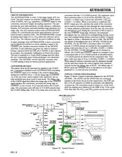
The equivalent circuit of the analog input section is shown in
Figure 11. During the acquisition interval the switches are both
in the track position and the AIN(+) charges the 20 pF capacitor
through the 125 Ω resistance. On the rising edge of CONVST
switches SW1 and SW2 go into the hold position retaining
charge on the 20 pF capacitor as a sample of the signal on
AIN(+). The AIN(–) is connected to the 20 pF capacitor, and
this unbalances the voltage at node A at the input of the com-
parator. The capacitor DAC adjusts during the remainder of the
conversion cycle to restore the voltage at node A to the correct
value. This action transfers a charge, representing the analog
input signal, to the capacitor DAC which in turn forms a digital
representation of the analog input signal. The voltage on the
AIN(–) pin directly influences the charge transferred to the
capacitor DAC at the hold instant. If this voltage changes dur-
ing the conversion period, the DAC representation of the analog
input voltage will be altered. Therefore it is most important that
the voltage on the AIN(–) pin remains constant during the conver-
sion period. Furthermore it is recommended that the AIN(–)
pin is always connected to AGND or to a fixed dc voltage.
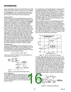
When no amplifier is used to drive the analog input the source
impedance should be limited to low values. The maximum
source impedance will depend on the amount of total harmonic
distortion (THD) that can be tolerated. The THD will increase
as the source impedance increases and performance will de-
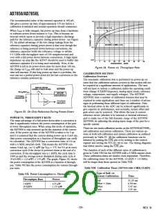
grade. Figure 12 shows a graph of the total harmonic distortion
versus analog input signal frequency for different source imped-
ances. With the setup as in Figure 13, the THD is at the –90 dB
level. With a source impedance of 1 kΩ and no capacitor on the
AIN(+) pin, the THD increases with frequency.
–72
THD vs. FREQUENCY FOR DIFFERENT
SOURCE IMPEDANCES
–76
R
= 1k⍀
IN
–80
–84
–88
–92
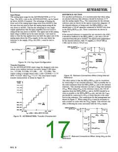
Acquisition Time
The track and hold amplifier enters its tracking mode on the
falling edge of the BUSY signal. The time required for the track
and hold amplifier to acquire an input signal will depend on
how quickly the 20 pF input capacitance is charged. The acqui-
sition time is calculated using the formula:
R
= 50⍀, 10nF
IN
AS IN FIGURE 13
0
20
40
60
80
100
tACQ = 9 ×(R +125 Ω)× 20 pF
IN
INPUT FREQUENCY – kHz
where RIN is the source impedance of the input signal, and
125 Ω, 20 pF is the input R, C.
Figure 12. THD vs. Analog Input Frequency
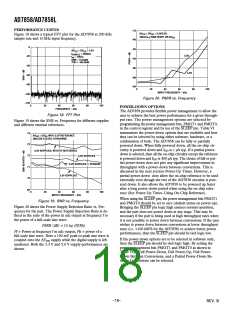
In a single supply application (both 3 V and 5 V), the V+ and
V– of the op amp can be taken directly from the supplies to the
AD7858/AD7858L which eliminates the need for extra external
power supplies. When operating with rail-to-rail inputs and
outputs, at frequencies greater than 10 kHz care must be taken
in selecting the particular op amp for the application. In particu-
lar for single supply applications the input amplifiers should be
connected in a gain of –1 arrangement to get the optimum per-
formance. Figure 13 shows the arrangement for a single supply
application with a 50 Ω and 10 nF low-pass filter (cutoff fre-
quency 320 kHz) on the AIN(+) pin. Note that the 10 nF is a
capacitor with good linearity to ensure good ac performance.
Recommended single supply op amps are the AD820 and the
AD820-3 V.
TRACK
125⍀
AIN(+)
SW1
HOLD
AIN(–)
125⍀
CAPACITOR
DAC
20pF
NODE A
SW2
COMPARATOR
HOLD
TRACK
C
REF2
Figure 11. Analog Input Equivalent Circuit
DC/AC Applications
For dc applications high source impedances are acceptable
provided there is enough acquisition time between conversions
to charge the 20 pF capacitor. The acquisition time can be
calculated from the above formula for different source imped-
ances. For example with RIN = 5 kΩ, the required acquisition
time will be 922 ns.
+3V TO +5V
10F
50⍀
0.1F
10k⍀
10k⍀
10k⍀
V
IN
)
V+
(0 TO V
TO AIN(+) OF
AD7858/AD7858L
REF
V
10nF
(NPO)
REF
AD820
AD820-3V
V+
10k⍀
Figure 13. Analog Input Buffering
–16–
REV. B

 ADI [ ADI ]