AD7858/AD7858L
Q. If a +20 mV offset is present in the analog input signal and the
reference voltage is 2.5 V what code needs to be written to the
offset register to compensate for the offset?
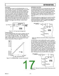
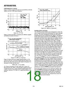
START
WRITE TO CONTROL REGISTER SETTING STCAL = 0, RDSLT1 = 1,
RDSLT0 = 0, AND CALSLT1, CALSLT0 = 00, 01, 10, 11
A. 2.5 V reference implies that the resolution in the offset regis-
ter is 5% × 2.5 V/213 = 0.015 mV. +20 mV/0.015 mV =
1310.72; rounding to the nearest number gives 1311. In
binary terms this is 0101 0001 1111. Therefore, decrease the
offset register by 0101 0001 1111.
CAL REGISTER POINTER IS
AUTOMATICALLY RESET
This method of compensating for offset in the analog input
signal allows for fine tuning the offset compensation. If the
offset on the analog input signal is known, there will be no need
to apply the offset voltage to the analog input pins and do a
system calibration. The offset compensation can take place in
software.
READ CAL REGISTER
CAL REGISTER POINTER IS
AUTOMATICALLY INCREMENTED
LAST
Adjusting the Gain Calibration Register
REGISTER
NO
READ
OPERATION
OR
ABORT
?
The gain calibration register contains 16 bits, two leading 0s
and 14 data bits. The data bits are binary weighted as in the
offset calibration register. The gain register value is effectively
multiplied by the analog input to scale the conversion result
over the full range. Increasing the gain register compensates for
a smaller analog input range and decreasing the gain register
compensates for a larger input range. The maximum analog
input range that the gain register can compensate for is 1.025
times the reference voltage, and the minimum input range is
0.975 times the reference voltage.
YES
FINISHED
Figure 9. Flowchart for Reading from the Calibration
Registers
Adjusting the Offset Calibration Register
The offset calibration register contains 16 bits, two leading zeros,
and 14 data bits. By changing the contents of the offset register
different amounts of offset on the analog input signal can be
compensated for. Increasing the number in the offset calibration
register compensates for negative offset on the analog input
signal, and decreasing the number in the offset calibration regis-
ter compensates for positive offset on the analog input signal.
The default value of the offset calibration register is 0010 0000
0000 0000 approximately. This is not an exact value, but the
value in the offset register should be close to this value. Each of
the 14 data bits in the offset register is binary weighted; the
MSB has a weighting of 5% of the reference voltage, the MSB-1
has a weighting of 2.5%, the MSB-2 has a weighting of 1.25%,
and so on down to the LSB which has a weighting of 0.0006%.
This gives a resolution of 0.0006% of VREF approximately.
More accurately the resolution is (0.05 × VREF )/213 volts =
0.015 mV, with a 2.5 V reference. The maximum offset that
can be compensated for is 5% of the reference voltage, which
equates to 125 mV with a 2.5 V reference and 250 mV with
a 5 V reference.
–14–
REV. B

 ADI [ ADI ]