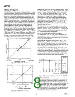
AD7769
Multichannel Expansion
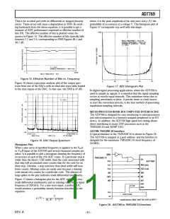
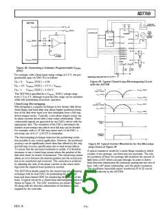
In some applications, more than two analog input channels are
required to be converted by the ADC. Figure 31 shows a circuit
configuration for such an application. T he ADG528A is a
latched, B-channel analog multiplexer that is ideally suited for
this application since it is specified for single supply operation
(+12 V ±10%).
T he CS, ADC/DAC and WR inputs of the AD7769 are gated to
drive the WR input of the ADG528A. T he multiplexer input
signal is selected on the falling edge of the WR pulse while the
signal is latched on the rising edge. Also, on the rising edge of
WR, the AD7769 ADC starts conversion. T herefore, the output
signal of the multiplexer must have settled to within 8-bits over
the duration of the WR pulse (see ADC Conversion Cycle sec-
tion for details). T he tON (WR) and settling time of the
ADG528A thus determines the width of the WR pulse.
Figure 31. Multichannel Inputs
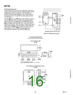
O UTLINE D IMENSIO NS
D imensions shown in inches and (mm).
28-Lead P lastic D IP
(N-28)
28-Lead P lastic Leaded Chip Car r ier
(P -28A)
REV. A
–16–

 ADI [ ADI ]