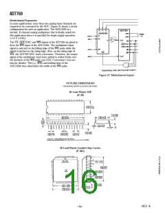
AD7769
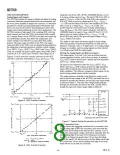
Incr eased Resolution D AC O utput
DAC A can be programmed to produce an interpolation func-
tion between the 8-bit steps of DAC B to allow, for example,
very smooth velocity profile waveforms to be generated.
Since both VBIAS (DAC) and VSWING (DAC) are common to
both output channels, the full-scale output voltages of both
channels are nominally identical. However, by adding an exter-
nal op amp and scaling resistors, it is possible to attenuate the
full-scale output voltage of one (or both) of the DAC outputs to
effectively increase the output voltage resolution. Figure 25
shows channel A being attenuated using a resistor scaling of
10:1. T he attenuated output voltage, VOUT A', is
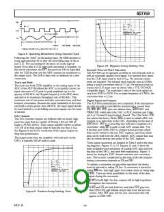
Ser vo O ffset Facility
Most dedicated servo disk drives offer an offset facility whereby
some small voltage is injected into the track-following loop. T he
purpose of the offset is to move the head to the right or left of its
current on-track position to permit reading of off-track data.
T he circuit is shown in Figure 27. With the 10:1 resistor scaling
used in the circuit the output voltage, VOUT , is
VOUTA' = VBIAS + (VSWING/10)(2DA–1).
VOUT = VPE + (VSWING/10) (2DA–1).
T he output voltage of Channel B remains at
VOUTB = VBIAS + VSWING (2DB–1).
DA and DB are fractional representations of the DAC input
codes, e.g., DA = NA/256 and DB = NB/256. For example, with a
VSWING voltage level of 2 V, the Channel B output span is 4 V
with an LSB size of 15.6 mV and (attenuated) Channel A out-
put span is 400 mV with an LSB size of 1.56 mV. Changing the
resistor scaling in Figure 25 obviously changes the attenuated
full-scale output.
Figure 27. Servo Offset Facility
With no offset added, VOUT = VPE, where VPE is the position
error voltage which the servo loop normally drives to its zero
level, VBIAS. When an offset voltage is supplied by DAC A, the
action of the servo is to move the head away from its current
on-track position until the position error voltage is equal and
opposite to the offset voltage. T he position of the head about
the track centre is thus programmable.
Figure 25. Increasing the DAC Output Voltage Resolution
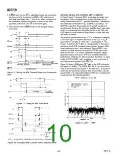
A single change to the circuit Figure 25 allows the two DAC
outputs to be combined to provide a single analog output with
resolution beyond the standard 8-bits. Figure 26 shows the rear-
ranged circuit. T he composite output, VOUT , is
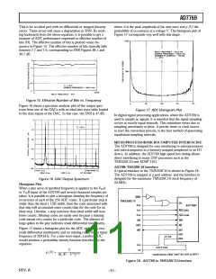
P r ogr am m able Full-Scale Range
T he output voltage span of both DACs is determined by the
VSWING (DAC) voltage level. T his is normally supplied from
some fixed voltage source. However, it is possible to use one of
the DAC channels to generate a programmable VSWING voltage
level. T he remaining channel will thus have a full-scale range
and LSB size which is software programmable. T his circuit is
shown in Figure 28 where VOUT B is used in an implicit feedback
loop to generate a programmable swing voltage, VSWING (DAC),
for the AD7769 from an external fixed input swing voltage,
VOUT = VOUTB + (VSWING/10)(2DA–1)
or
VOUT = VBIAS + VSWING (2DB–1) + (VSWING/10) (2DA–1).
VSWING. Using the 5:1 resistor scaling shown in Figure 28, the
expression for the AD7669 input swing voltage is
VSWING
.
VSWING (DAC) =
2D –1
(
)
B
1–
5
Figure 26. Com bined VOUTA, VOUTB Circuit
REV. A
–14–

 ADI [ ADI ]