AD7715
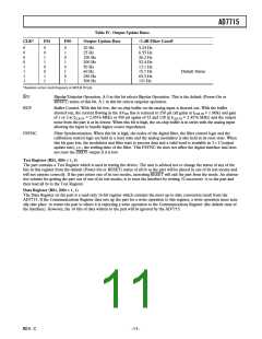
PIN FUNCTION DESCRIPTION
Pin No. Mnemonic
Function
1
2
3
4
5
SCLK
Serial Clock. Logic Input. An external serial clock is applied to this input to access serial data from
the AD7715. This serial clock can be a continuous clock with all data transmitted in a continuous
train of pulses. Alternatively, it can be a noncontinuous clock with the information being transmit-
ted to the AD7715 in smaller batches of data.
MCLK IN
MCLK OUT
CS
Master Clock signal for the device. This can be provided in the form of a crystal/resonator or exter-
nal clock. A crystal/resonator can be tied across the MCLK IN and MCLK OUT pins. Alterna-
tively, the MCLK IN pin can be driven with a CMOS-compatible clock and MCLK OUT left
unconnected. The part is specified with clock input frequencies of both 1 MHz and 2.4576 MHz.
When the master clock for the device is a crystal/resonator, the crystal/resonator is connected be-
tween MCLK IN and MCLK OUT. If an external clock is applied to MCLK IN, MCLK OUT
provides an inverted clock signal. This clock can be used to provide a clock source for external
circuitry.
Chip Select. Active low Logic Input used to select the AD7715. With this input hardwired low, the
AD7715 can operate in its three-wire interface mode with SCLK, DIN and DOUT used to inter-
face to the device. CS can be used to select the device in systems with more than one device on the
serial bus or as a frame synchronization signal in communicating with the AD7715.
RESET
Logic Input. Active low input which resets the control logic, interface logic, calibration coefficients,
digital filter and analog modulator of the part to power-on status.
6
7
8
9
AVDD
Analog Positive Supply Voltage, +3.3 V nominal (AD7715-3) or +5 V nominal (AD7715-5).
Analog Input. Positive input of the programmable gain differential analog input to the AD7715.
Analog Input. Negative input of the programmable gain differential analog input to the AD7715.
AIN(+)
AIN(–)
REF IN(+)
Reference Input. Positive input of the differential reference input to the AD7715. The reference
input is differential with the provision that REF IN(+) must be greater than REF IN(–).
REF IN(+) can lie anywhere between AVDD and AGND.
10
11
12
REF IN(–)
AGND
Reference Input. Negative input of the differential reference input to the AD7715. The REF IN(–)
can lie anywhere between AVDD and AGND provided REF IN(+) is greater than REF IN(–).
Ground reference point for analog circuitry. For correct operation of the AD7715, no voltage on
any of the other pins should go more than 30 mV negative with respect to AGND.
DRDY
Logic Output. A logic low on this output indicates that a new output word is available from the
AD7715 data register. The DRDY pin will return high upon completion of a read operation of a full
output word. If no data read has taken place between output updates, the DRDY line will return
high for 500 × tCLK IN cycles prior to the next output update. While DRDY is high, a read operation
should not be attempted or in progress to avoid reading from the data register as it is being updated.
The DRDY line will return low again when the update has taken place. DRDY is also used to indi-
cate when the AD7715 has completed its on-chip calibration sequence.
13
14
DOUT
DIN
Serial Data Output with serial data being read from the output shift register on the part. This output
shift register can contain information from the setup register, communications register or data regis-
ter depending on the register selection bits of the Communications Register.
Serial Data Input with serial data being written to the input shift register on the part. Data from this
input shift register is transferred to the setup register or communications register depending on the
register selection bits of the Communications Register.
15
16
DVDD
Digital Supply Voltage, +3.3 V or +5 V nominal.
Ground reference point for digital circuitry.
DGND
REV. C
–7–

 ADI [ ADI ]