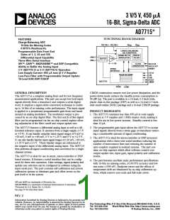
AD7715
(AV = +3 V, DV = +3 V, REF IN (+) = +1.25 V;
REF IN(–) = AGND; fCLK IN = 2.4576 MHz unless otherwise noted. All specifications TMIN to TMAX unless otherwise noted.)
AD7715-3–SPECIFICATIONS
DD
DD
Parameter
A Version1
Unit
Conditions/Comments
STATIC PERFORMANCE
No Missing Codes
16
Bits min
Guaranteed by Design. Filter Notch ≤ 60 Hz
Depends on Filter Cutoffs and Selected Gain
Filter Notch ≤ 60 Hz
Output Noise
See Tables IX to XII
Integral Nonlinearity
Unipolar Offset Error
Unipolar Offset Drift3
Bipolar Zero Error
±0.0015
See Note 2
0.2
See Note 2
0.2
See Note 2
0.2
See Note 2
0.2
% of FSR max
µV/°C typ
µV/°C typ
µV/°C typ
Bipolar Zero Drift3
Positive Full-Scale Error4
Full-Scale Drift3, 5
Gain Error6
Gain Drift3, 7
ppm of FSR/°C typ
% of FSR max
µV/°C typ
Bipolar Negative Full-Scale Error2
Bipolar Negative Full-Scale Drift3
±0.003
1
0.6
Typically ±0.0004%
For Gains of 1 and 2
For Gains of 32 and 128
µV/°C typ
ANALOG INPUTS/REFERENCE INPUTS
Input Common-Mode Rejection (CMR)
Normal-Mode 50 Hz Rejection8
Normal-Mode 60 Hz Rejection8
Common-Mode 50 Hz Rejection8
Common-Mode 60 Hz Rejection8
Common-Mode Voltage Range9
Absolute AIN/REF IN Voltage8
Specifications for AIN and REF IN Unless Noted
at DC. Typically 102 dB
90
98
98
150
dB min
dB min
dB min
dB min
dB min
V min to V max
V min
V max
V min
V max
For Filter Notches of 25 Hz, 50 Hz, ± 0.02 × fNOTCH
For Filter Notches of 20 Hz, 60 Hz, ± 0.02 × fNOTCH
For Filter Notches of 25 Hz, 50 Hz, ± 0.02 × fNOTCH
For Filter Notches of 20 Hz, 60 Hz, ± 0.02 × fNOTCH
AIN for BUF Bit of Setup Register = 0 and REF IN
AIN for BUF Bit of Setup Register = 0 and REF IN
150
AGND to AVDD
AGND – 30 mV
AVDD + 30 mV
AGND + 50 mV
AVDD – 1.5 V
1
Absolute/Common-Mode AIN Voltage9
BUF Bit of Setup Register = 1
AIN DC Input Current8
nA max
pF max
nom
AIN Sampling Capacitance8
AIN Differential Voltage Range10
10
0 to +VREF/GAIN11
±VREF/GAIN
GAIN × fCLK IN/64
Unipolar Input Range (B/U Bit of Setup Register = 1)
Bipolar Input Range (B/U Bit of Setup Register = 0)
For Gains of 1 and 2
nom
AIN Input Sampling Rate, fS
f
CLK IN/8
For Gains of 32 and 128
REF IN(+) – REF IN(–) Voltage
REF IN Input Sampling Rate, fS
+1.25
fCLK IN/64
V nom
±1% for Specified Performance. Functional with Lower VREF
LOGIC INPUTS
Input Current
±10
µA max
All Inputs Except MCLK IN
V
V
INL, Input Low Voltage
INH, Input High Voltage
0.8
2.0
V max
V min
MCLK IN Only
V
INL, Input Low Voltage
0.4
2.5
V max
V min
VINH, Input High Voltage
LOGIC OUTPUTS (Including MCLK OUT)
VOL, Output Low Voltage
0.4
DVDD – 0.6
±10
V max
V min
µA max
pF typ
ISINK = 100 µA Except for MCLK OUT12
ISOURCE = 100 µA Except for MCLK OUT12
VOH, Output High Voltage
Floating State Leakage Current
Floating State Output Capacitance13
Data Output Coding
9
Binary
Offset Binary
Unipolar Mode
Bipolar Mode
–3–
REV. C

 ADI [ ADI ]