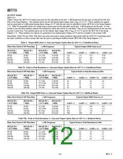
AD7715
Positive Full-Scale Overrange
TERMINOLOGY
Positive full-scale overrange is the amount of overhead available
to handle input voltages on AIN(+) input greater than AIN(–) +
VREF/GAIN (for example, noise peaks or excess voltages due to
system gain errors in system calibration routines) without intro-
ducing errors due to overloading the analog modulator or over-
flowing the digital filter.
Integral Nonlinearity
This is the maximum deviation of any code from a straight line
passing through the endpoints of the transfer function. The end-
points of the transfer function are Zero-Scale (not to be confused
with Bipolar Zero), a point 0.5 LSB below the first code transition
(000 . . . 000 to 000 . . . 001) and Full-Scale, a point 0.5 LSB
above the last code transition (111 . . . 110 to 111 . . . 111). The
error is expressed as a percentage of full scale.
Negative Full-Scale Overrange
This is the amount of overhead available to handle voltages on
AIN(+) below AIN(–) –VREF/GAIN without overloading the
analog modulator or overflowing the digital filter. Note that the
analog input will accept negative voltage peaks even in the uni-
polar mode provided that AIN(+) is greater than AIN(–) and
greater than AGND – 30 mV.
Positive Full-Scale Error
Positive Full-Scale Error is the deviation of the last code transi-
tion (111 . . . 110 to 111 . . . 111) from the ideal AIN(+) voltage
(AIN(–) + VREF/GAIN –3/2 LSBs). It applies to both unipolar
and bipolar analog input ranges.
Offset Calibration Range
Unipolar Offset Error
In the system calibration modes, the AD7715 calibrates its
offset with respect to the analog input. The offset calibration
range specification defines the range of voltages that the
AD7715 can accept and still calibrate offset accurately.
Unipolar Offset Error is the deviation of the first code transition
from the ideal AIN(+) voltage (AIN(–) + 0.5 LSB) when oper-
ating in the unipolar mode.
Bipolar Zero Error
Full-Scale Calibration Range
This is the range of voltages that the AD7715 can accept in the
system calibration mode and still calibrate full scale correctly.
This is the deviation of the midscale transition (0111 . . . 111
to 1000 . . . 000) from the ideal AIN(+) voltage (AIN(–)
– 0.5 LSB) when operating in the bipolar mode.
Input Span
Gain Error
In system calibration schemes, two voltages applied in sequence
to the AD7715’s analog input define the analog input range.
The input span specification defines the minimum and maxi-
mum input voltages from zero to full scale that the AD7715 can
accept and still calibrate gain accurately.
This is a measure of the span error of the ADC. It includes full-
scale errors but not zero-scale errors. For unipolar input ranges
it is defined as (full scale error–unipolar offset error) while for
bipolar input ranges it is defined as (full-scale error–bipolar zero
error).
Bipolar Negative Full-Scale Error
This is the deviation of the first code transition from the ideal
AIN(+) voltage (AIN(–) – VREF/GAIN + 0.5 LSB), when oper-
ating in the bipolar mode.
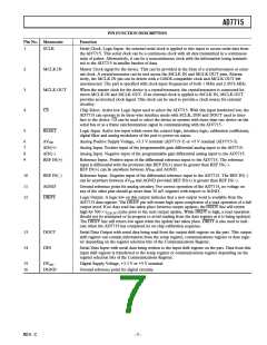
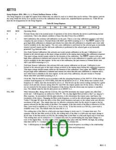
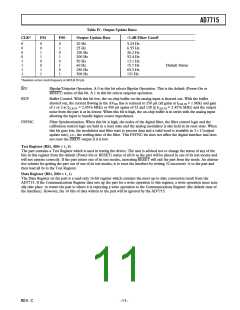
ON-CHIP REGISTERS
The part contains four on-chip registers which can be accessed by via the serial port on the part. The first of these is a Communica-
tions Register that decides whether the next operation is a read or write operation and also decides which register the read or write
operation accesses. All communications to the part must start with a write operation to the Communications Register. After power-
on or RESET, the device expects a write to its Communications Register. The data written to this register determines whether the
next operation to the part is a write or a read operation and also determines to which register this read or write operation occurs.
Therefore, write access to any of the other registers on the part starts with a write operation to the Communications Register fol-
lowed by a write to the selected register. A read operation from any register on the part (including the Communications Register itself
and the output data register) starts with a write operation to the Communications Register followed by a read operation from the
selected register. The Communication Register also controls the standby mode and the operating gain of the part. The DRDY status
is also available by reading from the Communications Register. The second register is a Setup Register that determines calibration
modes, filter selection and bipolar/unipolar operation. The third register is the Data Register from which the output data from the
part is accessed. The final register is a Test Register that is accessed when testing the device. It is advised that the user does not
attempt to access or change the contents of the test register as it may lead to unspecified operation of the device. The registers are
discussed in more detail in the following sections.
REV. C
–8–

 ADI [ ADI ]