AD7715
Communications Register (RS1, RS0 = 0, 0)
The Communications Register is an eight-bit register from which data can either be read or to which data can be written. All com-
munications to the part must start with a write operation to the Communications Register. The data written to the Communications
Register determines whether the next operation is a read or write operation and to which register this operation takes place. Once the
subsequent read or write operation to the selected register is complete, the interface returns to where it expects a write operation to
the Communications Register. This is the default state of the interface, and on power-up or after a RESET, the AD7715 is in this
default state waiting for a write operation to the Communications Register. In situations where the interface sequence is lost, if a
write operation to the device of sufficient duration (containing at least 32 serial clock cycles) takes place with DIN high, the AD7715
returns to this default state. Table I outlines the bit designations for the Communications Register.
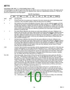
Table I. Communications Register
0/DRDY
ZERO
RS1
RS0
R/W
STBY
G1
G0
0/DRDY
For a write operation, a 0 must be written to this bit so that the write operation to the Communications Reg-
ister actually takes place. If a 1 is written to this bit, the part will not clock on to subsequent bits in the regis-
ter. It will stay at this bit location until a 0 is written to this bit. Once a 0 is written to this bit, the next 7 bits
will be loaded to the Communications Register. For a read operation, this bit provides the status of the
DRDY flag from the part. The status of this bit is the same as the DRDY output pin.
ZERO
For a write operation, a 0 must be written to this bit for correct operation of the part. Failure to do this will
result in unspecified operation of the device. For a read operation, a 0 will be read back from this bit location.
RS1– RS0
Register Selection Bits. These bits select to which one of four on-chip registers the next read or write opera-
tion takes place as shown in Table II along with the register size. When the read or write to the selected regis-
ter is complete, the part returns to where it is waiting for a write operation to the Communications Register.
It does not remain in a state where it will continue to access the selected register.
R/W
Read/Write Select. This bit selects whether the next operation is a read or write operation to the selected
register. A 0 indicates a write cycle as the next operation to the appropriate register, while a 1 indicates a read
operation from the appropriate register.
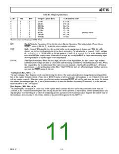
Table II. Register Selection
RS1
RS0
Register
Register Size
0
0
1
1
0
1
0
1
Communications Register
Setup Register
Test Register
8 Bits
8 Bits
8 Bits
16 Bits
Data Register
STBY
Standby. Writing a 1 to this bit puts the part in its standby or power-down mode. In this mode, the part
consumes only 10 µA of power supply current. The part retains its calibration and control word information
when in STANDBY. Writing a 0 to this bit places the part in its normal operating mode. The default value
for this bit after power-on or RESET is 0.
G2
0
0
G1
0
1
Gain Setting
1
2
1
1
0
1
32
128
REV. C
–9–

 ADI [ ADI ]