AD7715
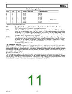
Table IV. Output Update Rates
Output Update Rate –3 dB Filter Cutoff
CLK*
FS1
FS0
0
0
0
0
1
1
1
1
0
0
1
1
0
0
1
1
0
1
0
1
0
1
0
1
20 Hz
25 Hz
100 Hz
200 Hz
50 Hz
60 Hz
250 Hz
500 Hz
5.24 Hz
6.55 Hz
26.2 Hz
52.4 Hz
13.1 Hz
15.7 Hz
65.5 Hz
131 Hz
Default Status
*Assumes correct clock frequency at MCLK IN pin
B/U
Bipolar/Unipolar Operation. A 0 in this bit selects Bipolar Operation. This is the default (Power-On or
RESET) status of this bit. A 1 in this bit selects unipolar operation.
BUF
Buffer Control. With this bit low, the on-chip buffer on the analog input is shorted out. With the buffer
shorted out, the current flowing in the AVDD line is reduced to 250 µA (all gains at fCLK IN = 1 MHz and gain
of 1 or 2 at fCLK IN = 2.4576 MHz) or 500 µA (gains of 32 and 128 @ fCLK IN = 2.4576 MHz) and the output
noise from the part is at its lowest. When this bit is high, the on-chip buffer is in series with the analog input
allowing the input to handle higher source impedances.
FSYNC
Filter Synchronization. When this bit is high, the nodes of the digital filter, the filter control logic and the
calibration control logic are held in a reset state and the analog modulator is also held in its reset state. When
this bit goes low, the modulator and filter start to process data and a valid word is available in 3 × 1/(output
update rate), i.e., the settling-time of the filter. This FSYNC bit does not affect the digital interface and does
not reset the DRDY output if it is low.
Test Register (RS1, RS0 = 1, 0)
The part contains a Test Register which is used in testing the device. The user is advised not to change the status of any of the
bits in this register from the default (Power-On or RESET) status of all 0s as the part will be placed in one of its test modes and
will not operate correctly. If the part enters one of its test modes, exercising RESET will exit the part from the mode. An alterna-
tive scheme for getting the part out of one of its test modes, is to reset the interface by writing 32 successive 1s to the part and
then load all 0s to the Test Register.
Data Register (RS1, RS0 = 1, 1)
The Data Register on the part is a read-only 16-bit register which contains the most up-to-date conversion result from the
AD7715. If the Communications Register data sets up the part for a write operation to this register, a write operation must actu-
ally take place to return the part to where it is expecting a write operation to the Communications Register (the default state of
the interface). However, the 16 bits of data written to the part will be ignored by the AD7715.
REV. C
–11–

 ADI [ ADI ]