AD7715
(DVDD = +3 V to +5.25 V; AVDD = +3 V to +5.25 V; AGND = DGND = 0 V; fCLKIN = 2.4576 MHz;
Input Logic 0 = 0 V, Logic 1 = DVDD, unless otherwise noted)
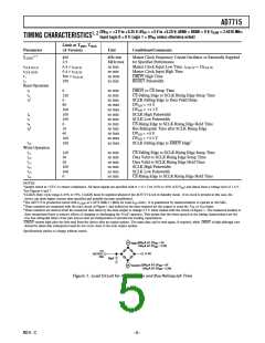
TIMING CHARACTERISTICS1, 2
Limit at TMIN, TMAX
Parameter
(A Version)
Unit
Conditions/Comments
3, 4
fCLKIN
400
2.5
0.4 × tCLK IN
0.4 × tCLK IN
500 × tCLK IN
100
kHz min
MHz max
ns min
ns min
ns nom
ns min
Master Clock Frequency: Crystal Oscillator or Externally Supplied
for Specified Performance
Master Clock Input Low Time. tCLK IN = 1/fCLK IN
Master Clock Input High Time
DRDY High Time
RESET Pulsewidth
tCLK IN LO
tCLK IN HI
t1
t2
Read Operation
t3
t4
t5
0
120
0
ns min
ns min
ns min
ns max
ns max
ns min
ns min
ns min
ns min
ns max
ns max
ns max
DRDY to CS Setup Time
CS Falling Edge to SCLK Rising Edge Setup Time
SCLK Falling Edge to Data Valid Delay
DVDD = +5 V
DVDD = +3.3 V
SCLK High Pulsewidth
5
80
100
100
100
0
10
60
t6
t7
t8
SCLK Low Pulsewidth
CS Rising Edge to SCLK Rising Edge Hold Time
Bus Relinquish Time after SCLK Rising Edge
DVDD = +5 V
6
t9
100
100
DVDD = +3.3 V
t10
SCLK Falling Edge to DRDY High7
Write Operation
t11
t12
t13
t14
t15
t16
120
30
20
100
100
0
ns min
ns min
ns min
ns min
ns min
ns min
CS Falling Edge to SCLK Rising Edge Setup Time
Data Valid to SCLK Rising Edge Setup Time
Data Valid to SCLK Rising Edge Hold Time
SCLK High Pulsewidth
SCLK Low Pulsewidth
CS Rising Edge to SCLK Rising Edge Hold Time
NOTES
1Sample tested at +25°C to ensure compliance. All input signals are specified with tr = tf = 5 ns (10% to 90% of D VDD) and timed from a voltage level of 1.6 V.
2See Figures 6 and 7.
3CLKIN Duty Cycle range is 45% to 55%. CLKIN must be supplied whenever the AD7715 is not in Standby mode. If no clock is present in this case, the
device can draw higher current than specified and possibly become uncalibrated.
4The AD7715 is production tested with fCLKIN at 2.4576 MHz (1 MHz for some IDD tests). It is guaranteed by characterization to operate at 400 kHz.
5These numbers are measured with the load circuit of Figure 1 and defined as the time required for the output to cross the VOL or VOH limits.
6These numbers are derived from the measured time taken by the data output to change 0.5 V when loaded with the circuit of Figure 1. The measured number is
then extrapolated back to remove effects of charging or discharging the 50 pF capacitor. This means that the times quoted in the timing characteristics are the
true bus relinquish times of the part and as such are independent of external bus loading capacitances.
7DRDY returns high after the first read from the device after an output update. The same data can be read again, if required, while DRDY is high although care
should be taken that subsequent reads do not occur close to the next output update.
Specifications subject to change without notice.
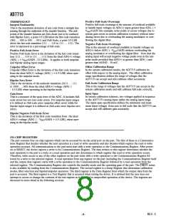
I
(800A AT DV = 5V
DD
SINK
100A AT DV = 3.3V)
DD
TO
OUTPUT
PIN
+1.6V
50pF
I
(200A AT DV = 5V
DD
SOURCE
100A AT DV = 3.3V)
DD
Figure 1. Load Circuit for Access Time and Bus Relinquish Time
REV. C
–5–

 ADI [ ADI ]