AD7715
CALIBRATION SEQUENCES
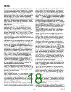
The AD7715 contains a number of calibration options as outlined previously. Table XIII summarizes the calibration types, the op-
erations involved and the duration of the operations. There are two methods of determining the end of calibration. The first is to
monitor when DRDY returns low at the end of the sequence. DRDY not only indicates when the sequence is complete but also that
the part has a valid new sample in its data register. This valid new sample is the result of a normal conversion which follows the cali-
bration sequence. The second method of determining when calibration is complete is to monitor the MD1 and MD0 bits of the
Setup Register. When these bits return to 0, 0 following a calibration command, it indicates that the calibration sequence is com-
plete. This method does not give any indication of there being a valid new result in the data register. However, it gives an earlier
indication than DRDY that calibration is complete. The duration to when the Mode Bits (MD1 and MD0) return to 0, 0 represents
the duration of the calibration carried out. The sequence to when DRDY goes low also includes a normal conversion and a pipeline
delay, tP, to correctly scale the results of this first conversion. tP will never exceed 2000 × tCLK IN. The time for both methods is given
in the table.
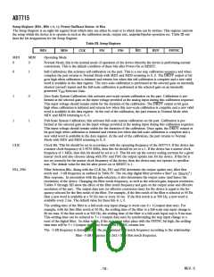
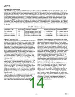
Table XIII. Calibration Sequences
Calibration Type
MD1, MD0 Calibration Sequence
Duration to Mode Bits Duration to DRDY
Self Calibration
0, 1
Internal ZS Cal @ Selected Gain + 6 × 1/Output Rate 9 × 1/Output Rate + tP
Internal FS Cal @ Selected Gain
ZS Cal on AIN @ Selected Gain
FS Cal on AIN @ Selected Gain
ZS System Calibration
FS System Calibration
1, 0
1, 1
3 × 1/Output Rate
3 × 1/Output Rate
4 × 1/Output Rate + tP
4 × 1/Output Rate + tP
CIRCUIT DESCRIPTION
information. The programmable gain function on the analog
input is also incorporated in this sigma-delta modulator with the
input sampling frequency being modified to give the higher
gains. A sinc3 digital low-pass filter processes the output of the
sigma-delta modulator and updates the output register at a rate
determined by the first notch frequency of this filter. The out-
put data can be read from the serial port randomly or periodi-
cally at any rate up to the output register update rate. The first
notch of this digital filter (and hence its –3 dB frequency) can be
programmed via the Setup Register bits FS0 and FS1. With a
master clock frequency of 2.4576 MHz, the programmable
range for this first notch frequency is from 50 Hz to 500 Hz
giving a programmable range for the –3 dB frequency of
13.1 Hz to 131 Hz. With a master clock frequency of 1 MHz,
the programmable range for this first notch frequency is from
20 Hz to 200 Hz giving a programmable range for the –3 dB
frequency of 5.24 Hz to 52.4 Hz.
The AD7715 is a sigma-delta A/D converter with on-chip digital
filtering, intended for the measurement of wide dynamic range,
low frequency signals such as those in industrial control or pro-
cess control applications. It contains a sigma-delta (or charge-
balancing) ADC, a calibration microcontroller with on-chip
static RAM, a clock oscillator, a digital filter and a bidirectional
serial communications port. The part consumes only 450 µA of
power supply current, making it ideal for battery-powered or
loop-powered instruments. The part comes in two versions, the
AD7715-5 which is specified for operation from a nominal
+5 V analog supply (AVDD) and the AD7715-3 which is speci-
fied for operation from a nominal +3.3 V analog supply. Both
versions can be operated with a digital supply (DVDD) voltage of
+3.3 V or +5 V.
The part contains a programmable-gain fully differential analog
input channel. The selectable gains on this input are 1, 2, 32
and 128 allowing the part to accept unipolar signals of between
0 mV to +20 mV and 0 V to +2.5 V or bipolar signals in the
range from ±20 mV to ±2.5 V when the reference input voltage
equals +2.5 V. With a reference voltage of +1.25 V, the input
ranges are from 0 mV to +10 mV to 0 V to +1.25 V in unipolar
mode and from ±10 mV to ±1.25 V in bipolar mode. Note that
the bipolar ranges are with respect to AIN(–) and not with re-
spect to AGND.
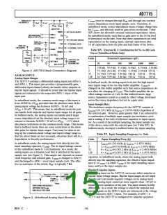
The basic connection diagram for the AD7715-5 is shown in
Figure 2. This shows both the AVDD and DVDD pins of the
AD7715 being driven from the analog +5 V supply. Some
applications will have AVDD and DVDD driven from separate
supplies. An AD780, precision +2.5 V reference, provides the
reference source for the part. On the digital side, the part is
configured for three-wire operation with CS tied to DGND. A
quartz crystal or ceramic resonator provides the master clock
source for the part. In most cases, it will be necessary to connect
capacitors on the crystal or resonator to ensure that it does
not oscillate at overtones of its fundamental operating fre-
quency. The values of capacitors will vary depending on the
manufacturer’s specifications.
The input signal to the analog input is continuously sampled at
a rate determined by the frequency of the master clock,
MCLK IN, and the selected gain. A charge-balancing A/D
converter (sigma-delta modulator) converts the sampled signal
into a digital pulse train whose duty cycle contains the digital
REV. C
–14–

 ADI [ ADI ]