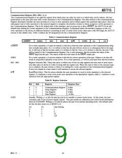
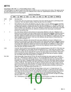
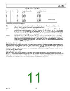
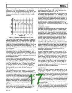
AD7715
AD7715-3
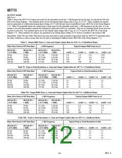
Table IX shows the AD7715-3 output rms noise for the selectable notch and –3 dB frequencies for the part, as selected by FS1 and
FS0 of the Setup Register. The numbers given are for the bipolar input ranges with a VREF of +1.25 V. These numbers are typical
and are generated at an analog input voltage of 0 V with the part used in unbuffered mode (BUF bit of the Setup Register = 0).
Table X meanwhile shows the output peak-to-peak noise for the selectable notch and –3 dB frequencies for the part. It is important to
note that these numbers represent the resolution for which there will be no code flicker. They are not calculated based on rms noise but on peak-
to-peak noise. The numbers given are for the bipolar input ranges with a VREF of +1.25 V and for the BUF bit of the Setup Register =
0. These numbers are typical, are generated at an analog input voltage of 0 V and are rounded to the nearest LSB.
Meanwhile, Table XI and Table XII show rms noise and peak-to-peak resolution respectively with the AD7715-3 operating under
the same conditions as above except that now the part is operating in buffered mode (BUF Bit of the Setup Register = 1).
Table IX. Output RMS Noise vs. Gain and Output Update Rate for AD7715-3 (Unbuffered Mode)
Filter First Notch & O/P Data Rate
–3 dB Frequency
Typical Output RMS Noise in V
MCLK IN =
2.4576 MHz
MCLK IN =
1 MHz
MCLK IN =
2.4576 MHz
MCLK IN =
1 MHz
GAIN = 1
GAIN = 2
GAIN = 32
GAIN = 128
50 Hz
60 Hz
250 Hz
500 Hz
20 Hz
25 Hz
100 Hz
200 Hz
13.1 Hz
15.72 Hz
65.5 Hz
131 Hz
5.24 Hz
6.55 Hz
26.2 Hz
52.4 Hz
3.0
3.4
45
1.7
2.1
20
0.7
0.7
2.2
9.7
0.65
0.7
1.6
3.3
270
135
Table X. Peak-to-Peak Resolution vs. Gain and Output Update Rate for AD7715-3 (Unbuffered Mode)
Filter First Notch & O/P Data Rate –3 dB Frequency Typical Peak-to-Peak Resolution in Bits
MCLK IN =
2.4576 MHz
MCLK IN =
1 MHz
MCLK IN =
2.4576 MHz
MCLK IN =
1 MHz
GAIN = 1
GAIN = 2
GAIN = 32
GAIN = 128
50 Hz
60 Hz
250 Hz
500 Hz
20 Hz
25 Hz
100 Hz
200 Hz
13.1 Hz
15.72 Hz
65.5 Hz
131 Hz
5.24 Hz
6.55 Hz
26.2 Hz
52.4 Hz
16
16
13
11
16
16
13
11
14
14
13
10
12
12
11
10
Table XI. Output RMS Noise vs. Gain and Output Update Rate for AD7715-3 (Buffered Mode)
Filter First Notch & O/P Data Rate –3 dB Frequency Typical Output RMS Noise in V
MCLK IN =
2.4576 MHz
MCLK IN =
1 MHz
MCLK IN =
2.4576 MHz
MCLK IN =
1 MHz
GAIN = 1
GAIN = 2
GAIN = 32
GAIN = 128
50 Hz
60 Hz
250 Hz
500 Hz
20 Hz
25 Hz
100 Hz
200 Hz
13.1 Hz
15.72 Hz
65.5 Hz
131 Hz
5.24 Hz
6.55 Hz
26.2 Hz
52.4 Hz
4.5
5.1
50
2.4
2.9
25
0.9
0.9
2.6
9.7
0.9
1.0
2
270
135
3.3
Table XII. Peak-to-Peak Resolution vs. Gain and Output Update Rate for AD7715-3 (Buffered Mode)
Filter First Notch & O/P Data Rate –3 dB Frequency Typical Peak-to-Peak Resolution in Bits
MCLK IN =
2.4576 MHz
MCLK IN =
1 MHz
MCLK IN =
2.4576 MHz
MCLK IN =
1 MHz
GAIN = 1
GAIN = 2
GAIN = 32
GAIN = 128
50 Hz
60 Hz
250 Hz
500 Hz
20 Hz
25 Hz
100 Hz
200 Hz
13.1 Hz
15.72 Hz
65.5 Hz
131 Hz
5.24 Hz
6.55 Hz
26.2 Hz
52.4 Hz
16
16
13
10
16
16
13
11
14
14
12
10
12
12
11
10
REV. C
–13–

 ADI [ ADI ]