AD7715
ANALOG
+5V SUPPLY
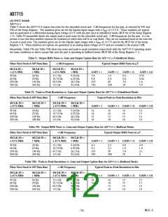
CSAMP must be charged through RSW and through any external
source impedances every input sample cycle. Therefore, in
unbuffered mode, source impedances mean a longer charge time
for CSAMP, and this may result in gain errors on the part. Table
XIV shows the allowable external resistance/capacitance values,
for unbuffered mode, such that no gain error to the 16-bit level
is introduced on the part. Note that these capacitances are total
capacitances on the analog input, external capacitance plus
10 pF capacitance from the pins and lead frame of the device.
10F
0.1F
0.1F
AV
DV
DD
DD
AD7715
DRDY
DATA READY
AIN(+)
AIN(–)
DIFFERENTIAL
ANALOG INPUT
CS
DOUT
DIN
RECEIVE (READ)
SERIAL DATA
ANALOG
GROUND
AGND
DGND
ANALOG
+5V SUPPLY
SCLK
RESET
SERIAL CLOCK
DIGITAL
GROUND
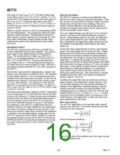
Table XIV. External R, C Combination for No 16-Bit Gain
Error (Unbuffered Mode Only)
+5V
V
IN
V
REF IN(+)
OUT
0.1F
10F
AD780
GND
Gain
External Capacitance (pF)
50 100 500 1000
MCLK IN
REF IN(–)
MCLK OUT
CRYSTAL OR
CERAMIC
RESONATOR
10
5000
1
2
32
128
152 kΩ 53.9 kΩ 31.4 kΩ 8.4 kΩ 4.76 kΩ 1.36 kΩ
75.1 kΩ 26.6 kΩ 15.4 kΩ 4.14 kΩ 2.36 kΩ 670 Ω
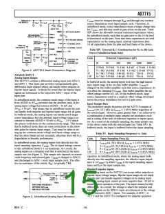
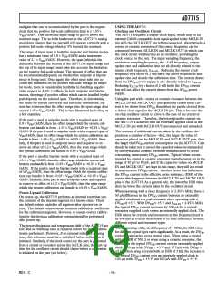
Figure 2. AD7715-5 Basic Connection Diagram
ANALOG INPUT
16.7 kΩ 5.95 kΩ 3.46 kΩ 924 Ω 526 Ω
16.7 kΩ 5.95 kΩ 3.46 kΩ 924 Ω 526 Ω
150 Ω
150 Ω
Analog Input Ranges
The AD7715 contains a differential analog input pair AIN(+)
and AIN(–). This input pair provides a programmable-gain,
differential input channel which can handle either unipolar or
bipolar input signals. It should be noted that the bipolar input
signals are referenced to the respective AIN(–) input of the
input pair.
In buffered mode, the analog inputs look into the high imped-
ance inputs stage of the on-chip buffer amplifier. CSAMP is
charged via this buffer amplifier such that source impedances do
not affect the charging of CSAMP. This buffer amplifier has an
offset leakage current of 1 nA. In this buffered mode, large
source impedances result in a small dc offset voltage developed
across the source impedance but not in a gain error.
In unbuffered mode, the common-mode range of the input is
from AGND to AVDD provided that the absolute value of the
analog input voltage lies between AGND – 30 mV and
AVDD + 30 mV. This means that in unbuffered mode the part
can handle both unipolar and bipolar input ranges for all gains.
In buffered mode, the analog inputs can handle much larger
source impedances but the absolute input voltage range is re-
stricted to between AGND + 50 mV to AVDD – 1.5 V which
also places restrictions on the common-mode range. This means
that in buffered mode there are some restrictions on the allow-
able gains for bipolar input ranges. Care must be taken in set-
ting up the common-mode voltage and input voltage range so
that the above limits are not exceeded, otherwise there will be a
degradation in linearity performance.
Input Sample Rate
The modulator sample frequency for the AD7715 remains at
fCLK IN/128 (19.2 kHz @ fCLK IN = 2.4576 MHz) regardless of
the selected gain. However, gains greater than 1 are achieved by
a combination of multiple input samples per modulator cycle
and a scaling of the ratio of reference capacitor to input capaci-
tor. As a result of the multiple sampling, the input sample rate
of the device varies with the selected gain (see Table XV). In
buffered mode, the input is buffered before the input sampling
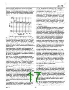
Table XV. Input Sampling Frequency vs. Gain
Gain
Input Sampling Freq (fS)
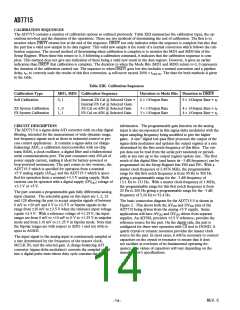
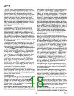
In unbuffered mode, the analog inputs look directly into the
input sampling capacitor, CSAMP. The dc input leakage current
in this unbuffered mode is 1 nA maximum. As a result, the
analog inputs see a dynamic load that is switched at the input
sample rate (see Figure 3). This sample rate depends on master
clock frequency and selected gain. CSAMP is charged to AIN(+)
and discharged to AIN(–) every input sample cycle. The effec-
tive on-resistance of the switch, RSW, is typically 7 kΩ.
1
2
32
128
f
CLK IN/64 (38.4 kHz @ fCLK IN = 2.4576 MHz)
2 × fCLK IN/64 (76.8 kHz @ fCLK IN = 2.4576 MHz)
8 × fCLK IN/64 (307.2 kHz @ fCLK IN = 2.4576 MHz)
8 × fCLK IN/64 (307.2 kHz @ fCLK IN = 2.4576 MHz)
capacitor. In unbuffered mode, where the analog input looks
directly into the sampling capacitor, the effective input imped-
ance is 1/CSAMP × fS where CSAMP is the input sampling capaci-
tance and fS is the input sample rate.
Bipolar/Unipolar Inputs
AIN(+)
The analog input on the AD7715 can accept either unipolar or
bipolar input voltage ranges. Bipolar input ranges do not imply
that the part can handle negative voltages on its analog input
since the analog input cannot go more negative than –30 mV to
ensure correct operation of the part. The input channel is fully
differential. As a result, the voltage to which the unipolar and
bipolar signals on the AIN(+) input are referenced is the voltage
on the respective AIN(–) input. For example, if AIN(–) is
+2.5 V and the AD7715 is configured for unipolar operation
R
(7k⍀ TYP)
HIGH
IMPEDANCE
1G⍀
SW
C
SAMP
AIN(–)
(10pF )
V
BIAS
SWITCHING FREQUENCY
DEPENDS ON fCLKIN
AND SELECTED GAIN
Figure 3. Unbuffered Analog Input Structure
REV. C
–15–

 ADI [ ADI ]