AD73360L
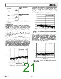
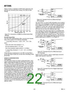
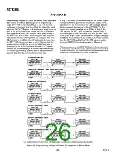
Figure 23 shows a comparison of SNR results achieved by vary-
ing either the Decimation Rate Setting or the DMCLK Rate
Settings.
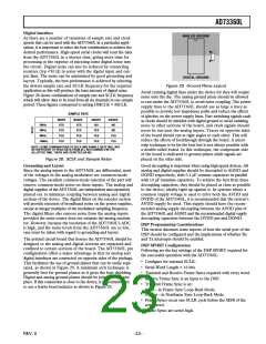
100⍀
100⍀
VINPx
VINNx
VIN
0.047F
0.047F
81
TO INPUT BIAS
CIRCUITRY
REFOUT
DMCLK = MCLK
80
VOLTAGE
REFERENCE
REFCAP
0.1F
79
78
77
76
Figure 24. Example Circuit for Differential Input
(DC Coupling)
The AD73360L’s on-chip 38 dB preamplifier can be enabled
when there is not enough gain in the input circuit; the preampli-
fier is configured by bits IGS0–2 of CRD. The total gain must be
configured to ensure that a full-scale input signal produces a
signal level at the input to the sigma-delta modulator of the
ADC that does not exceed the maximum input range.
REDUCED
75
DMCLK
74
73
72
71
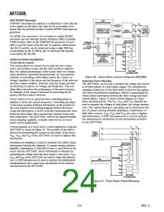
The dc biasing of the analog input signal is accomplished with
an on-chip voltage reference. If the input signal is not biased at
the internal reference level (via REFOUT), then it must be
ac-coupled with external coupling capacitors. CIN should be
0.1 µF or larger. The dc biasing of the input can then be accom-
plished using resistors to REFOUT as in Figure 25.
8
16
24
32
40
48
56
64
SAMPLING FREQUENCY – kHz
Figure 23. Comparison of DMCLK and Decimation Rate
Settings
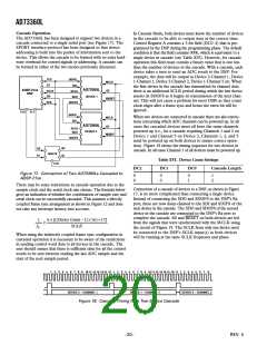
Encoder Group Delay
The AD73360L implementation offers a very low level of group
delay, which is given by the following relationship:
CIN
100⍀
100⍀
VINPx
VINNx
Group Delay (Decimator) = Order × ((M – 1)/2) × Tdec
where:
10k⍀
10k⍀
VIN
CIN
0.047F
Order is the order of the decimator (= 3),
M is the decimation factor (= 32), and
Tdec is the decimation sample interval (= 1/2.048e6).
0.047F
TO INPUT BIAS
CIRCUITRY
REFOUT
VOLTAGE
REFERENCE
REFCAP
0.1F
=> Group Delay (Decimator) = 3 × (32 – 1)/2 × (1/2.048e6)
= 22.7 µs
Figure 25. Example Circuit for Differential Input
(AC Coupling)
If final filtering is implemented in the DSP, the final filter’s
group delay must be taken into account when calculating overall
group delay.
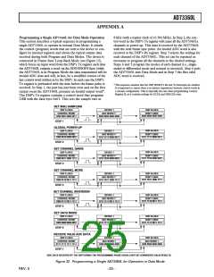
Figures 26 and 27 detail ac- and dc-coupled input circuits for
single-ended operation respectively.
DESIGN CONSIDERATIONS
Analog Inputs
CIN
100⍀
VINPx
VINNx
VIN
10k⍀
The AD73360L features six signal conditioning inputs. Each
signal conditioning block allows the AD73360L to be used with
either a single-ended or differential signal. The applied signal
can also be inverted internally by the AD73360L if required.
The analog input signal to the AD73360L can be dc-coupled,
provided that the dc bias level of the input signal is the same as
the internal reference level (REFOUT). Figure 24 shows the
recommended differential input circuit for the AD73360L. The
circuit of Figure 24 implements first-order low-pass filters
with a 3 dB point at 34 kHz; these are the only filters that must
be implemented external to the AD73360L to prevent aliasing
of the sampled signal. Since the ADC uses a highly oversampled
approach that transfers the bulk of the antialiasing filtering into
the digital domain, the off-chip antialiasing filter need only be of
a low order. It is recommended that for optimum performance the
capacitors used for the antialiasing filter be of high-quality
dielectric (NPO).
0.047F
REFOUT
VOLTAGE
REFERENCE
REFCAP
0.1F
Figure 26. Example Circuit for Single-Ended Input
(AC Coupling)
100⍀
VINPx
VINNx
VIN
0.047F
REFOUT
VOLTAGE
REFERENCE
REFCAP
0.1F
Figure 27. Example Circuit for Differential Input
(DC Coupling)
–22–
REV. 0

 ADI [ ADI ]