AD694
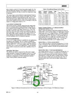
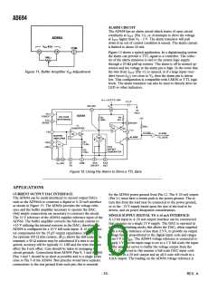
ALARM CIRCUIT
The AD694 has an alarm circuit which warns of open circuit
conditions at IOUT (Pin 11), or of attempts to drive the voltage
at IOUT higher than VS – 2 V. The alarm transistor will pull
down if an out of control condition is sensed. The alarm current
is limited to about 20 mA.
Figure 12 shows a typical application. In a digital/analog system
the alarm can provide a TTL signal to a controller. The collec-
tor of the alarm transistor is tied to the system logic supply
through a 20 kΩ pull-up resistor. The alarm is off in normal op-
eration and the voltage at the alarm pin is high. In the event that
the wire from IOUT (Pin 11) is opened, or if a large input over-
drive forces IOUT too close to VS, then the alarm pin is driven
low. This configuration is compatible with CMOS or TTL logic
levels. The alarm transistor can also be used to directly drive an
LED or other indicators.
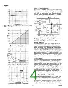
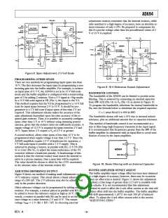
Figure 11. Buffer Amplifier VOS Adjustment
Figure 12. Using the Alarm to Drive a TTL Gate
APPLICATIONS
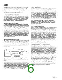
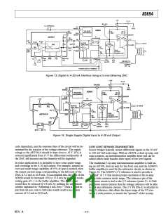
CURRENT OUTPUT DAC INTERFACE
for the AD566 power ground from Pin 12. The 4–20 mA output
(Pin 11) must have a return path to the power ground. The re-
turn line from the load may be connected to the power ground,
or to the –15 V supply based upon the size of the load to be
driven, and on power dissipation considerations.
The AD694 can be easily interfaced to current output DACs
such as the AD566A to construct a digital to 4–20 mA interface
as shown in Figure 13. The AD694 provides the voltage refer-
ence and the buffer amplifier necessary to operate the DAC.
Only simple connections are necessary to construct the circuit.
The 10 V reference of the AD694 supplies reference input of the
AD566. The buffer amplifier converts the full-scale current to
+10 V utilizing the internal resistors in the DAC; therefore the
AD694 is configured for a 10 V full-scale input. A 10 pF capaci-
tor compensates for the 25 pF output capacitance of the DAC.
An optional 100 Ω trim resistor, (RT), allows the full-scale to be
trimmed, a 50 Ω resistor may be substituted if a trim is not re-
quired; accuracy will be typically ±1 LSB and the trim does not
affect the 4 mA offset. Care should be taken in managing the
circuit grounds. Connections from AD694 Pins 9, 3 and AD566
Pins 3 and 7 should be as short as possible and to a single point
close to Pin 5 of the AD694. Best practice would have separate
connections to the star ground from each pin; this is essential
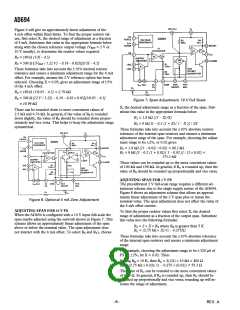
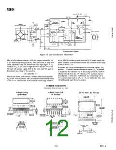
SINGLE SUPPLY DIGITAL TO 4–20 mA INTERFACE
A 12 bit input to 4–20 mA output interface can be constructed
that operates on a single 15 V supply. The DAC is operated in
its voltage switching mode; this allows the DAC, when supplied
with a voltage reference of less than 2.5 V, to provide an output
voltage that is proportional to the digital input code and ranges
from 0 V to VREF. The AD694 voltage reference is connected to
supply 2 V and the input stage is set to a 2 V full scale; the input
buffer amplifier serves to buffer the voltage output from the
DAC. Connected in this manner a full-scale DAC input code
will result in a 20 mA output and an all 0 code will result in a
4 mA output. The loading on the AD694 voltage reference is
–10–
REV. A

 ADI [ ADI ]