AD694
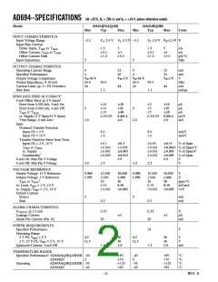
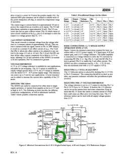
Table I. Precalibrated Ranges for the AD694
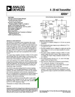
drive a load to a point 36 V below the positive supply (VS). An
optional NPN pass transistor can be added to transfer most of
the power dissipation off-chip, to extend the temperature range
of operation.
I
nput
Output
Range
Voltage
Reference VS
Min
Range
Pin 9 Pin 4 Pin 8
The output stage is current-limited at approximately 38 mA to
protect the output from an overdrive at its inputs. The V/I will
allow linear operation to approximately 24 mA. The V/I con-
verter also has an open collector alarm (Pin 10) which warns of
open-circuit condition at the IOUT pin or of attempts to drive the
output to a voltage greater than VS –2 V.
0–2 V
0–10 V
0–2.5 V
0–12.5 V 0–20 mA 2 V
0–2 V
0–10 V
0–2.5 V
0–12.5 V 0–20 mA 10 V
4–20 mA 2 V
4–20 mA 2 V
0–20 mA 2 V
4.5 V
Pin 5 Pin 5 Pin 7
12.5 V Pin 5 Open Pin 7
5.0 V ≥3 V Pin 5 Pin 7
15.0 V ≥3 V Open Pin 7
12.5 V Pin 5 Pin 5 Open
12.5 V Pin 5 Open Open
12.5 V ≥3 V Pin 5 Open
15.0 V ≥3 V Open Open
4–20 mA 10 V
4–20 mA 10 V
0–20 mA 10 V
4 mA OFFSET GENERATOR
This circuit converts a constant voltage from the voltage refer-
ence to a constant current of approximately 200 µA. This cur-
rent is summed with the signal current at Pin 14 (BW Adjust),
to result in a constant 4 mA offset current at IOUT. The 4 mA
Adj (Pin 6) allows the offset current to be adjusted to any cur-
rent in the range of 2 mA to 4.8 mA. Pin 9 (4 mA On/Off) can
shut off the offset current completely if it is lifted to 3.0 V or
more, allowing 0 to 20 mA operation of the AD694. In normal
4-20 mA operation, Pin 9 is connected to ground.
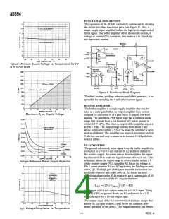
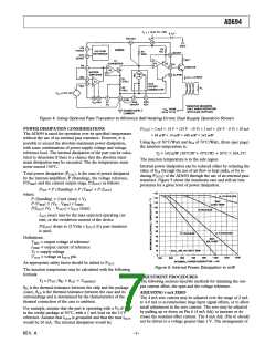
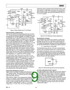
BASIC CONNECTIONS: 12.5 V SINGLE SUPPLY
OPERATION WITH 10 V FS
Figure 2 shows the minimal connections required for basic op-
eration with a +12.5 V power supply, 10 V input span, 4-20 mA
output span, and a 10 V voltage reference. The buffer amplifier
is connected as a voltage follower to drive the V/I converter by
connecting FB (Pin 1) to –Sig (Pin 2). 4 mA On/Off (Pin 9) is
tied to ground (Pin 5) to enable the 4 mA offset current. The
AD694 can drive a maximum load RL = [VS – 2 V] /20 mA,
thus the maximum load with a 12.5 V supply is 525 Ω.
VOLTAGE REFERENCE
A 2 V or 10 V voltage reference is available for user applications,
selectable by pin-strapping. The 10 V option is available for
supply voltages greater than 12.5 V, the 2 V output is available
over the whole 4.5 V – 36 V power supply range. The reference
can source up to 5 mA for user applications. A boost transistor
can be added to increase the current drive capability of the 2 V
mode.
SELECTING A 2 V FULL-SCALE INPUT
The 2 V full-scale option is selected by shorting Pin 4 (2 V FS)
to Pin 5 (Common). The connection should be as short as pos-
sible; any parasitic resistance will affect the precalibrated span
accuracy.
SELECTING THE 2 V VOLTAGE REFERENCE
The voltage reference is set to a 2 V output by shorting Pin 7 to
Pin 8 (10 V Force to 2 V Sense). If desired, the 2 V reference
can be set up for remote force and sense connection. Keep in
mind that the 2 V Sense line carries a constant current of 100µA
that could cause an offset error over long wire runs. The 2 V
reference option can be used with all supply voltages greater
than 4.5 V.
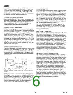
APPLYING THE AD694
The AD694 can easily be connected for either dual or single
supply operation, to operate from supplies as low as 4.5 V and
as high as 36 V. The following sections describe the different
connection configurations, as well as adjustment methods.
Table I shows possible connection options.
Figure 2. Minimal Connections for 0-10 V Single-Ended Input, 4-20 mA Output, 10 V Reference Output
–5–
REV. A

 ADI [ ADI ]