AD694
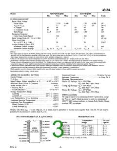
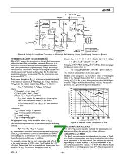
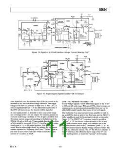
Figure 4. Using Optional Pass Transistor to Minimize Self-Heating Errors; Dual Supply Operation Shown
POWER DISSIPATION CONSIDERATIONS
P(TOT) = 2 mA × 24 V + (24 V – 10 V) × 1 mA + (24 V – 0 V) × 20 mA
The AD694 is rated for operation over its specified temperature
without the use of an external pass transistor. However, it is
possible to exceed the absolute maximum power dissipation,
with some combinations of power supply voltage and voltage
reference load. The internal dissipation of the part can be calcu-
lated to determine if there is a chance that the absolute maxi-
mum dissipation may be exceeded. The die temperature must
never exceed 150°C.
= 48 mW + 14 mW + 480 mW = 542 mW
Using θJC of 30°C/Watt and θCA of 70°C/Watt, (from spec page)
the junction temperature is:
TJ = 542 mW (30°C/W + 70°C/W) + 50°C = 104.2°C
The junction temperature is in the safe region.
Internal power dissipation can be reduced either by reducing the
value of θCA through the use of air flow or heat sinks, or by re-
ducing P(TOT) of the AD694 through the use of an external pass
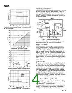
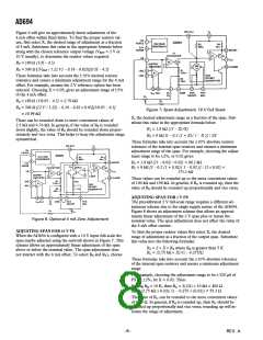
transistor. Figure 5 shows the maximum case and still air tem-
peratures for a given level of power dissipation.
Total power dissipation (PTOT), is the sum of power dissipated
by the internal amplifiers, P (Standing), the voltage reference,
P(VREF) and the current output stage, P(IOUT) as follows:
PTOT = P (Standing) + P (VREF) + P (IOUT
)
where:
P (Standing) = 2 mA (max) × VS
P (VREF) = (VS – VREF) × IVREF
P(IOUT) (VS – VOUT) × IOUT (max):
I
OUT (max) may be the max expected operating cur-
rent, or the overdriven current of the device.
P(IOUT) drops to (2 Volts × IOUT) if a pass transistor
is used.
Definitions:
REF = output voltage of reference
VREF = output current of reference
VS = supply voltage
OUT = voltage at IOUT pin.
V
I
V
An appropriate safety factor should be added to PTOT
.
Figure 5. Internal Power Dissipation in mW
The junction temperature may be calculated with the following
formula:
ADJUSTMENT PROCEDURES
The following sections describe methods for trimming the out-
put current offset, the span and the voltage reference.
TJ = PTOT (θJC + θCA) + TAMBIENT
θJC is the thermal resistance between the chip and the package
(case), θCA is the thermal resistance between the case and its
surroundings and is determined by the characteristics of the
thermal connection of the case to ambient.
ADJUSTING 4 mA ZERO
The 4 mA zero current may be adjusted over the range of 2 mA
to 4.8 mA to accommodate large input signal offsets, or to allow
small adjustment in the zero current. The zero may be adjusted
by pulling up or down on Pin 6 (4 mA Adj) to increase or de-
crease the nominal offset current. The 4 mA Adj. (Pin 6) should
not be driven to a voltage greater than 1 V. The arrangement of
For example, assume that the part is operating with a VS of 24 V
in the cerdip package at 50°C, with a 1 mA load on the 10 V
reference. Assume that IOUT is grounded and that the max IOUT
would be 20 mA. The internal dissipation would be:
REV. A
–7–

 ADI [ ADI ]