AD694
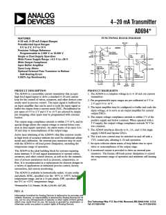
FUNCTIONAL DESCRIPTION
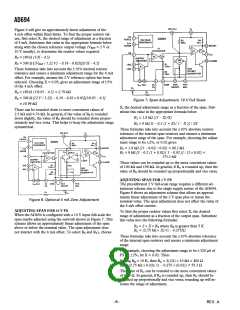
The operation of the AD694 can best be understood by dividing
the circuit into three functional parts (see Figure 1). First, a
single supply input amplifier buffers the high level, single-ended
input signal. The buffer amplifier drives the second section, a
voltage to current (V/I) converter, that makes a 0 to 16 mA sig-
nal dependent current.
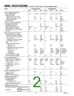
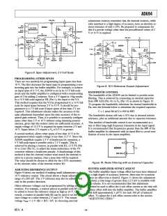
Typical Minimum Supply Voltage vs. Temperature for 2 V
& 10 V Full Scale
Figure 1. Functional Block Diagram
The third section, a voltage reference and offset generator, is re-
sponsible for providing the 4 mA offset current signal.
BUFFER AMPLIFIER
The buffer amplifier is a single supply amplifier that may be
used as a unity gain buffer, an output amplifier for a current
output D/A converter, or as a gain block to amplify low level
signals. The amplifier’s PNP input stage has a common-mode
range that extends from a few hundred mV below ground to
within 2.5 V of VS. The Class A output of the amplifier appears
at Pin 1 (FB). The output range extends from about 1 mV
above common to within 2.5 V of VS when the amplifier is oper-
ated as a follower. The amplifier can source a maximum load of
5 kΩ, but can sink only as much as its internal 10 kΩ pulldown
resistor allows.
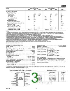
Maximum RL vs. Supply Voltage
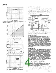
Voltage Reference Power Supply Rejection
IOUT: Voltage Compliance vs. Temperature
V/I CONVERTER
The ground referenced, input signal from the buffer amplifier is
converted to a 0 to 0.8 mA current by A2 and level shifted to
the positive supply. A current mirror then multiplies this signal
by a factor of 20 to make the signal current of 0 to 16 mA. This
technique allows the output stage to drive a load to within 2 V
of the positive supply (VS). Amplifier A2 forces the voltage at
Pin 1 across resistors R1 and R2 by driving the Darlington tran-
sistor, Q2. The high gain Darlington transmits the resistor cur-
rent to its collector and to R3 (900 Ω). A3 forces the level
shifted signal across the 45 Ω resistor to get a current gain of 20.
The transfer function of the V/I stage is therefore:
IOUT = 20 × V(PIN1 / R1 + R2
(
)
)
resulting in a 0-16 mA output swing for a 0–10 V input. Tying
Pin 4 (2 V FS) to ground shorts out R2 and results in a 2 V
full-scale input for a 16 mA output span.
The output stage of the V/I converter is of a unique design that
allows the IOUT pin to drive a load below the common (sub-
strate) potential of the device. The output transistor can always
–4–
REV. A

 ADI [ ADI ]