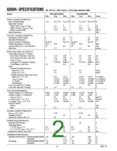
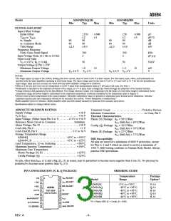
AD694
An NPN boost transistor can be added in the 2 V mode to in-
crease the current drive capability of the 2 V reference. The
10 V force pin is connected to the base of the NPN, and the
NPN emitter is connected to the 2 V sense pin. The minimum
VS Of the part increases by approximately 0.7 V.
0-20 mA OPERATION
A 0-20 mA output range is available with the AD694 by remov-
ing the 4 mA offset current with the 4 mA On/Off pin. In nor-
mal 4-20 mA operation 4 mA On/Off (Pin 9) is tied to ground,
enabling the 4 mA offset current. Tying Pin 9 to a potential of
3 V or greater turns off the 4 mA offset current; connecting Pin
9 to the 10 V reference, the positive supply, or a TTL control
pin, is a convenient way to do this. In 0–20 mA mode the input
span is increased by 20%, thus the precalibrated input spans of
2 V and 10 V become 2.5 V and 12.5 V. Minimum supply volt-
ages for the two spans increase to 5 V and 15 V.
4.5 V SINGLE SUPPLY OPERATION
For operation with a +4.5 V power supply, the input span and
the voltage reference output must be reduced to give the ampli-
fiers their required 2.5 V of head room for operation. This is
done by adjusting the AD694 for 2 V full-scale input, and a
voltage reference output of 2 V as described above.
The 4 mA On/Off pin may also be used as a “jiggle pin” to
unstick valves or actuators, or as a way to shut off a 4–20 mA
loop entirely. Note that the pin only removes the 4 mA offset
and not the signal current.
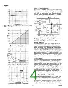
GENERAL DESIGN GUIDELINES
A 0.1 µF decoupling capacitor is recommended in all applica-
tions from VS (Pin 13) to Com (Pin 5). Additional components
may be required if the output load is nonresistive, see section on
driving nonresistive loads. The buffer amplifier PNP inputs
should not be brought more than –0.3 V of common, or they
will begin to source large amounts of current. Input protection
resistors must be added to the inputs if there is a danger of this
occurring. The output of the buffer amplifier, Pin 1 (FB), is not
short circuit protected. Shorting this pin to ground or VS with a
signal present on the amplifier may damage it. Input signals
should not drive Pin 1 (FB) directly; always use the buffer am-
plifier to buffer input signals.
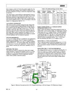
DUAL SUPPLY OPERATION
Figure 4 shows the AD694 operated in dual supply mode. (Note
that the pass transistor is shown for illustration and is not re-
quired for dual supply operation.) The device is powered com-
pletely by the positive supply which may be as low as 4.5 V. The
unique design of the output stage allows the IOUT pin to extend
below common to a negative supply. The output stage can
source a current to a point 36 V below the positive supply. For
example, when operated with a +12.5 V supply, the AD694 can
source a current to a point as low as 23.5 V below common.
This feature can simplify the interface to dual supply D/A con-
verters by eliminating grounding and level-shifting problems
while increasing the load that the transmitter is able to drive.
Note that the IOUT pin is the only pin that should be allowed to
extend lower than –0.3 V of common.
DRIVING NONRESISTIVE LOADS
The AD694 is designed to be stable when driving resistive loads.
Adding a 0.01 µF capacitor from IOUT (Pin 11) to Com (Pin 5),
as shown in Figure 3, insures the stability of the AD694 when
driving inductive or poorly defined loads. This capacitor is rec-
ommended when there is any uncertainty as to the characteris-
tics of the load.
OPERATION WITH A PASS TRANSISTOR
The AD694 can operate as a stand-alone 4–20 mA converter
with no additional active components. However, provisions have
been made to connect IOUT to the base of an external NPN pass
transistor as shown in Figure 4. This permits a majority of the
power dissipation to be moved off-chip to enhance performance
and extend the temperature range of operation. Note that the
positive output voltage compliance is reduced by approximately
0.7 V, the VBE of the pass device. A 50 Ω resistor should be
added in series with the pass transistor collector, when the
AD694 is operated with dual supplies, as shown in Figure 4.
This will not reduce the voltage compliance of the output stage.
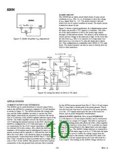
Figure 3. Capacitor Utilized When Driving Nonresistive
Loads; Protection Diodes Used When Driving Inductive
Loads
The external pass transistor selected should have a BVCEO
greater than the intended supply voltage with a sufficient power
rating for continuous operation with 25 mA current at the sup-
ply voltage. Ft should be in the 10 MHz to 100 MHz range and
β should be greater than 10 at a 20 mA emitter current. Heat
sinking the external pass transistor is suggested.
Additional protection is recommended when driving inductive
loads. Figure 3 shows two protective diodes, D1 and D2, added
to protect against voltage spikes that may extend above VS or
below common that could damage the AD694. These diodes
should be used in addition to the 0.01 µF capacitor. When the
optional NPN transistor is used, the capacitor and diodes
should connect to the NPN emitter instead of Pin 11.
–6–
REV. A

 ADI [ ADI ]