AD549
100µ
10µ
1µ
I
–
IN
I
+
IN
100n
10n
1n
100p
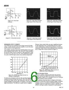
Figure 39. Input Voltage Clamp with Diodes
10p
1p
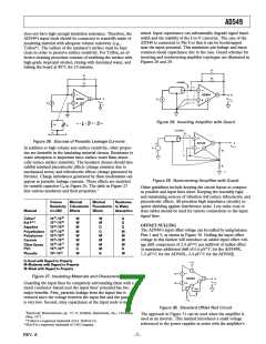
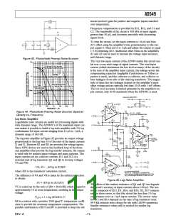
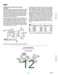
SAMPLE AND DIFFERENCE CIRCUIT TO MEASURE
ELECTROMETER LEAKAGE CURRENTS
100f
10f
There are a number of methods used to test electrometer leak-
age currents, including current integration and direct current to
voltage conversion. Regardless of the method used, board and
interconnect cleanliness, proper choice of insulating materials
(such as Teflon or Kel-F), correct guarding and shielding tech-
niques and care in physi-cal layout are essential to making accu-
rate leakage measurements.
–5 –4 –3 –2 –1
0
1
2
3
4
5
–
–
)
DIFFERENTIAL INPUT VOLTAGE – V (V
– V
IN
IN
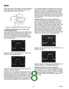
Figure 36. Input Current vs. Differential Input Voltage
INPUT PROTECTION
The AD549 safely handles any input voltage within the supply
voltage range. Subjecting the input terminals to voltages beyond
the power supply can destroy the device or cause shifts in input
current or offset voltage if the amplifier is not protected.
Figure 40 is a schematic of the sample and difference circuit. It
uses two AD549 electrometer amplifiers (A and B) as current-to
voltage converters with high value (1010 Ω) sense resistors (RSa
and RSb). R1 and R2 provide for an overall circuit sensitivity of
10 fA/mV (10 pA full scale). CC and CF provide noise suppres-
sion and loop compensation. CC should be a low leakage poly-
styrene capacitor. An ultralow leakage Kel-F test socket is used
for contacting the device under test. Rigid Teflon coaxial cable
is used to make connections to all high impedance nodes. The
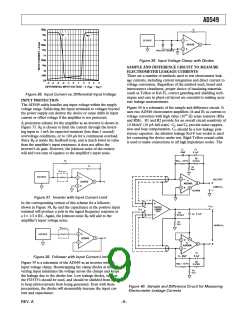
A protection scheme for the amplifier as an inverter is shown in
Figure 37. RP is chosen to limit the current through the invert-
ing input to 1 mA for expected transient (less than 1 second)
overvoltage conditions, or to 100 µA for a continuous overload.
Since RP is inside the feedback loop, and is much lower in value
than the amplifier’s input resistance, it does not affect the
inverter’s dc gain. However, the Johnson noise of the resistor
will add root sum of squares to the amplifier’s input noise.
Figure 37. Inverter with Input Current Limit
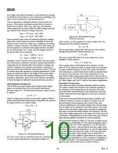
In the corresponding version of this scheme for a follower,
shown in Figure 38, RP and the capacitance at the positive input
terminal will produce a pole in the signal frequency response at
a f = 1/2 π RC. Again, the Johnson noise RP will add to the
amplifier’s input voltage noise.
Figure 38. Follower with Input Current Limit
Figure 39 is a schematic of the AD549 as an inverter with an
input voltage clamp. Bootstrapping the clamp diodes at the in-
verting input minimizes the voltage across the clamps and keeps
the leakage due to the diodes low. Low leakage diodes, such as
the FD333’s should be used, and should be shielded from light
to keep photocurrents from being generated. Even with these
precautions, the diodes will measurably increase the input cur-
rent and capacitance.
Figure 40. Sample and Difference Circuit for Measuring
Electrometer Leakage Currents
REV. A
–9–

 ADI [ ADI ]