AD549
mized. Input capacitance can substantially degrade signal band-
width and the stability of the I-to-V converter. The case of the
AD549 is connected to Pin 8 so that it can be bootstrapped
near the input potential. This minimizes pin leakage and input
common-mode capacitance due to the case. Guard schemes for
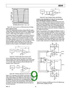
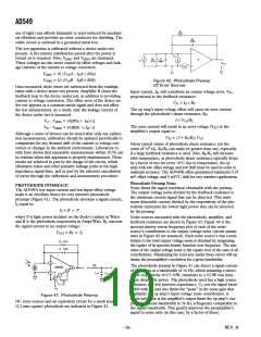
inverting and noninverting amplifier topologies are illustrated in
Figures 28 and 29.
does not have high enough insulation resistance. Therefore, the
AD549’s input leads should be connected to standoffs made of
insulating material with adequate volume resistivity (e.g.,
Teflon*). The surface of the insulator’s surface must be kept
clean in order to preserve surface resistivity. For Teflon, an ef-
fective cleaning procedure consists of swabbing the surface with
high-grade isopropyl alcohol, rinsing with deionized water, and
baking the board at 80°C for 10 minutes.
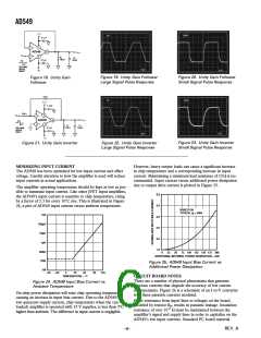
Figure 28. Inverting Amplifier with Guard
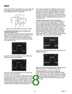
Figure 26. Sources of Parasitic Leakage Currents
In addition to high volume and surface resistivity, other proper-
ties are desirable in the insulating material chosen. Resistance to
water absorption is important since surface water films drasti-
cally reduce surface resistivity. The insulator chosen should also
exhibit minimal piezoelectric effects (charge emission due to
mechanical stress) and triboelectric effects (charge generated by
friction). Charge imbalances generated by these mechanisms can
appear as parasitic leakage currents. These effects are modeled
by variable capacitor CP in Figure 26. The table in Figure 27
lists various insulators and their properties.1
Figure 29. Noninverting Amplifier with Guard
Other guidelines include keeping the circuit layout as compact
as possible and input lines short. Keeping the assembly rigid
and minimizing sources of vibration will reduce triboelectric and
piezoelectric effects. All precision high impedance circuitry re-
quires shielding against interference noise. Low noise coax or
triax cables should be used for remote connections to the input
signal lines.
Volume
Minimal
Minimal
Resistance
Resistivity Triboelectric Piezoelectric to Water
Material
(⍀–CM)
Effects
Effects
Absorption
Teflon*
Kel-F**
1017–1018
1017–1018
1016–1018
1014–1018
1012–1018
1012–1014
1010–1017
1010–1015
105–1012
W
W
M
M
W
W
W
G
W
M
G
G
G
G
M
M
W
W
G
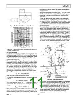
OFFSET NULLING
Sapphire
Polyethylene
Polystyrene
Ceramic
Glass Epoxy
PVC
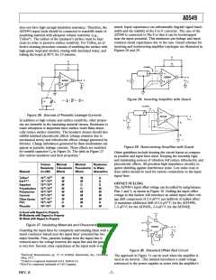
The AD549’s input offset voltage can be nulled by usingbalance
Pins 1 and 5, as shown in Figure 30. Nulling the input offset
voltage in this fashion will introduce an added input offset volt-
age drift component of 2.4 µV/°C per millivolt of nulled offset
(a maximum additional drift of 0.6 µV/°C for the AD549K,
1.2 µV/°C for the AD549L, 2.4 µV/°C for the AD549J).
G
M
M
M
M
G
Phenolic
W
W
G–Good with Regard to Property
M–Moderate with Regard to Property
W–Weak with Regard to Property
Figure 27. Insulating Materials and Characteristics
Guarding the input lines by completely surrounding them with a
metal conductor biased near the input lines’ potential has two
major benefits. First, parasitic leakage from the signal line is
reduced since the voltage between the input line and the guard
is very low. Second, stray capacitance at the input node is mini-
Figure 30. Standard Offset Null Circuit
1Electronic Measurements, pp. 15–17, Keithley Instruments, Inc., Cleveland,
Ohio, 1977.
*Teflon is a registered trademark of E.I. DuPont Co.
**Kel-F is a registered trademark of 3-M Company.
The approach in Figure 31 can be used when the amplifier is
used as an inverter. This method introduces a small voltage
referenced to the power supplies in series with the amplifier’s
REV. A
–7–

 ADI [ ADI ]