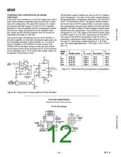
AD549
positive input terminal. The amplifier’s input offset voltage drift
with temperature is not affected. However, variation of the
power supply voltages will cause offset shifts.
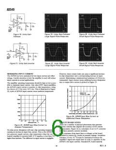
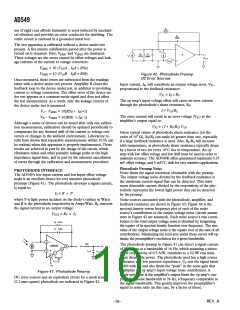
In an inverting configuration, the differential input capacitance
forms a pole in the circuit’s loop transmission. This can create
peaking in the ac response and possible instability. A feedback
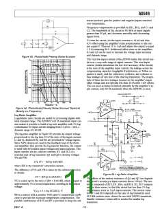
capacitance can be used to stabilize the circuit. The inverter
pulse response with RF and RS equal to 1 MΩ appears in Figure
34. Figure 35 shows the response of the same circuit with a I pF
feedback capacitance. Typical differential input capacitance for
the AD549 is 1 pF.
COMMON-MODE INPUT VOLTAGE OVERLOAD
The rated common-mode input voltage range of the AD549 is
from 3 V less than the positive supply voltage to 5 V greater
than the negative supply voltage. Exceeding this range will de-
grade the amplifier’s CMRR. Driving the common-mode voltage
above the positive supply will cause the amplifier’s output to
saturate at the upper limit of output voltage. Recovery time is
typically 2 µs after the input has been returned to within the nor-
mal operating range. Driving the input common-mode voltage
within 1 V of the negative supply causes phase reversal of the
output signal. In this case, normal operation is typically resumed
within 0.5 µs of the input voltage returning within range.
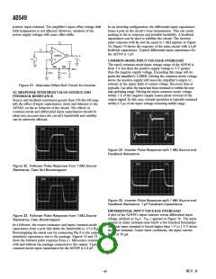
Figure 31. Alternate Offset Null Circuit for Inverter
AC RESPONSE WITH HIGH VALUE SOURCE AND
FEEDBACK RESISTANCE
Source and feedback resistances greater than 100 kΩ will mag-
nify the effect of input capacitances (stray and inherent to the
AD549) on the ac behavior of the circuit. The effects of
common-mode and differential input capacitances should be
taken into account since the circuit’s bandwidth and stability
can be adversely affected.
Figure 34. Inverter Pulse Response with 1 MΩ Source and
Feedback Resistance
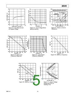
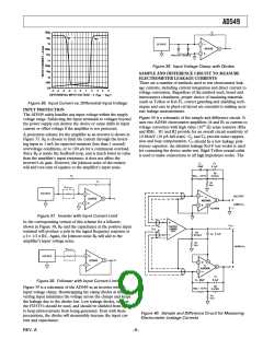
Figure 32. Follower Pulse Response from 1 MΩ Source
Resistance, Case Not Bootstrapped
Figure 35. Inverter Pulse Response with 1 MΩ Source and
Feedback Resistance, 1 pF Feedback Capacitance
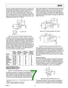
DIFFERENTIAL INPUT VOLTAGE OVERLOAD
A plot of the AD549’s input currents versus differential input
voltage (defined as VIN+ –VIN–) appears in Figure 36. The input
current at either terminal stays below a few hundred femtoamps
until one input terminal is forced higher than 1 V to 1.5 V above
the other terminal. Under these conditions, the input current
limits at 30 µA.
Figure 33. Follower Pulse Response from 1 MΩ Source
Resistance, Case Bootstrapped
In a follower, the source resistance and input common-mode
capacitance form a pole that limits the bandwidth to 1/2 π RSCS.
Bootstrapping the metal case by connecting Pin 8 to the output
minimizes capacitance due to the package. Figures 32 and 33
show the follower pulse response from a 1 MΩ source resistance
with and without the package connected to the output. Typical
common-mode input capacitance for the AD549 is 0.8 pF.
–8–
REV. A

 ADI [ ADI ]