AD549
use of rigid coax affords immunity to error induced by mechani-
cal vibration and provides an outer conductor for shielding. The
entire circuit is enclosed in a grounded metal box.
The test apparatus is calibrated without a device under test
present. A five minute stabilization period after the power is
turned on is required. First, VERR1 and VERR2 are measured.
These voltages are the errors caused by offset voltages and leak-
age currents of the current to voltage converters.
VERR1 = 10 (VOSA – IBA × RSa)
VERR2 = 10 (VOSB – IBB × RSb)
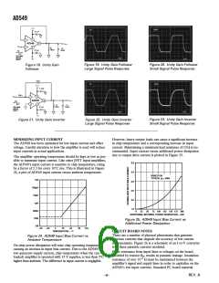
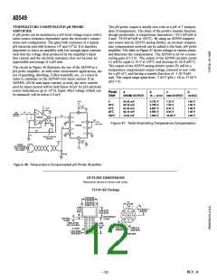
Figure 42. Photodiode Preamp
DC Error Sources
Once measured, these errors are subtracted from the readings
taken with a device under test present. Amplifier B closes the
feedback loop to the device under test, in addition to providing
current to voltage conversion. The offset error of the device un-
der test appears as a common-mode signal and does not affect
the test measurement. As a result, only the leakage current of
the device under test is measured.
Input current, IB, will contribute an output voltage error, VE1,
proportional to the feedback resistance:
VE1 = IB × RF
The op amp’s input voltage offset will cause an error current
through the photodiode’s shunt resistance, RS:
I = VOS/RS
VA – VERR1 = 10[RSa × IB(+)]
VX – VERR2 = 10[RSb × IB(–)]
The error current will result in an error voltage (VE2) at the
amplifier’s output equal to:
Although a series of devices can be tested after only one calibra-
tion measurement, calibration should be updated periodically to
compensate for any thermal drift of the current to voltage con-
verters or changes in the ambient environment. Laboratory re-
sults have shown that repeatable measurements within 10 fA can
be realized when this apparatus is properly implemented. These
results are achieved in part by the design of the circuit, which
eliminates relays and other parasitic leakage paths in the high
impedance signal lines, and in part by the inherent cancellation
of errors through the calibration and measurement procedure.
VE2 = ( I + RF/RS) VOS
Given typical values of photodiode shunt resistance (on the
order of 109 Ω), RF/RS can easily be greater than one, especially
if a large feedback resistance is used. Also, RF/RS will increase
with temperature, as photodiode shunt resistance typically drops
by a factor of two for every 10°C rise in temperature. An op
amp with low offset voltage and low drift must be used in order to
maintain accuracy. The AD549K offers guaranteed maximum 0.25
mV offset voltage, and 5 mV/°C drift for very sensitive applications.
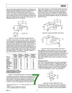
Photodiode Preamp Noise
PHOTODIODE INTERFACE
Noise limits the signal resolution obtainable with the preamp.
The output voltage noise divided by the feedback resistance is
the minimum current signal that can be detected. This mini-
mum detectable current divided by the responsivity of the pho-
todiode represents the lowest light power that can be detected
by the preamp.
The AD549’s low input current and low input offset voltage
make it an excellent choice for very sensitive photodiode
preamps (Figure 41). The photodiode develops a signal current,
IS equal to:
IS = R × P
where P is light power incident on the diode’s surface in Watts
and R is the photodiode responsivity in Amps/Watt. RF converts
the signal current to an output voltage:
Noise sources associated with the photodiode, amplifier, and
feedback resistance are shown in Figure 43; Figure 44 is the
spectral density versus frequency plot of each of the noise
source’s contribution to the output voltage noise (circuit param-
eters in Figure 42 are assumed). Each noise source’s rms contri-
bution to the total output voltage noise is obtained by integrating
the square of its spectral density function over frequency. The rms
value of the output voltage noise is the square root of the sum of all
contributions. Minimizing the total area under these curves will op-
timize the preamplifier’s resolution for a given bandwidth.
V
OUT = RF × IS
The photodiode preamp in Figure 41 can detect a signal current
of 26 fA rms at a bandwidth of 16 Hz, which assuming a photo-
diode responsivity of 0.5 A/W, translates to a 52 fW rms mini-
mum detectable power. The photodiode used has a high source
resistance and low junction capacitance. CF sets the signal band-
width with RF and also limits the “peak” in the noise gain that
multiplies the op amp’s input voltage noise contribution. A
single pole filter at the amplifier’s output limits the op amp’s out-
put voltage noise bandwidth to 26 Hz, a frequency comparable to
the signal bandwidth. This greatly improves the preamplifier’s
signal to noise ratio (in this case, by a factor of three).
Figure 41. Photodiode Preamp
DC error sources and an equivalent circuit for a small area
(0.2 mm square) photodiode are indicated in Figure 42.
–10–
REV. A

 ADI [ ADI ]